PLC concepts
4.2 Data storage, memory areas, I/O and addressing
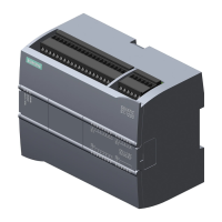
S7-1200 Programmable controller
System Manual, 03/2014, A5E02486680-AG
109
Table 4- 24 Absolute addressing for DB memory
Bit DB[data block number].DBX[byte
DB1.DBX2.3
Byte, Word, or Double
DB[data block number].DB [size][starting
DB1.DBB4, DB10.DBW2,
Note
When you specify an absolute address in LAD or FBD, STEP 7 precedes this address with a
"%" character to indicate that it is an absolute address. While programming, you can enter
an absolute address either with or witho
ut the "%" character (for example %I0.0 or I.0). If
7 supplies the "%" character.
In SCL, you must enter the "%" before the address to indicate that it is an absolute address.
Without the "%", STEP
7 generates an undefined tag error at compile time
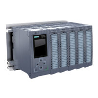
Configuring the I/O in the CPU and I/O modules
When you add a CPU and I/O modules to your
configuration screen, I and Q ad
dresses are
automatically assigned. You can change the
default addressing by selecting the address field in
the device configuration and typing new numbers.
Digital inputs and outputs are assigned in
groups of 8 points (1 byte), whether the module
uses all the points or not.
Analog inputs and outputs are assigned in
groups of 2 points (4 bytes).
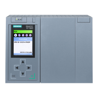
The figure shows an example of a CPU 1214C with two SMs and one SB. In this example,
you could change the address of the DI8 module to 2 instead of 8. The tool assists you by
changing address ranges that are the wrong size or conflict with other addresses.
 Loading...