Although the I C. sockets do not need to go any particular way round, you may like to put the bevelled
corner at the notch end of the I.C. position as a reminder, since the semicircie printed on the board will
be covered by the socket in some cases.
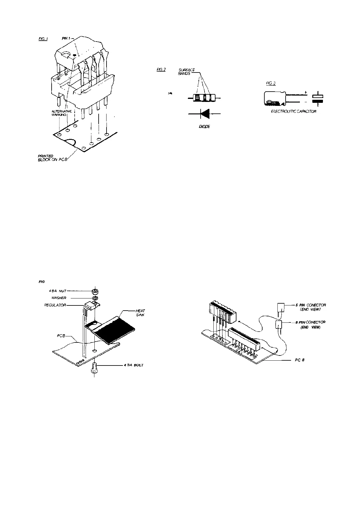
(b) The diodes (prefix D) have their + end identified by the band painted on the body - or in the case of
components with several bands, the + end will be the widest band. This corresponds to the flat bar of
the symbol printed on the board. (See fig. 2).
(c) The electrolytic capacitors (C3 & C5}will have a + or - symbol printed on them, and the + wire is
usually longer. (See fig. 3).
(d) The transistors (prefix TR) go in the board as shown by the picture printed at their positions - i.e.
with their rounded corners facing the edge connector.
(e) The jack sockets and modulator need to have their business ends (i.e. where the plug goes in)
facing outwards, away from the components. This should be obvious by inspection of the board and
case.
(f) The regulator (REG) and heatsink need to go in a particular way round -just follow fig. 4.
(g) The keyboard connectors KB1 & KB2 have their pins offset from their centre line, and KB1 goes
the opposite way round to KB2. Make sure that in each case the body of the connector covers up the
component number on the board. (See fig. 5). . , . ... ... ..-,... . ,. . ..
(h)
The
resistor packs
(prefix
RP)
have
a
'common'
end
marked wltn
a
whlte
dot
Thls snould
9°
at tne
end marked with a 'C' on the board.
(i) The single resistors, the rest of the capacitors, and the filter X1 may be put in either way round.

 Loading...