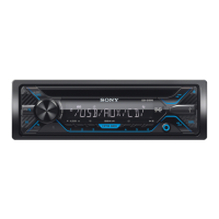
CDX-G1200U/G1201U/G1202U/G1280UM
30
MAIN BOARD IC1305 LC78615E-01US-H (RF AMP, DIGITAL SERVO PROCESSOR)
Pin No. Pin Name I/O Description
1 EFMIN I RF signal input terminal
2 RFOUT O RF signal output terminal
3 LPF - External low-pass fi lter capacitor connection terminal for DC level detection of RF signal
4 PHLPF - External low-pass fi lter capacitor connection terminal for defect detection
5 AIN I Main beam (B) input from the CD mechanism deck block
6 CIN I Main beam (C) input from the CD mechanism deck block
7 BIN I Main beam (A) input from the CD mechanism deck block
8 DIN I Main beam (C) input from the CD mechanism deck block
9 SLCISET - External resistor connection terminal for current setting of SLCO output
10 RFMON O Internal analog signal monitor terminal of LSI Not used
11 VREF O Reference voltage (+1.65V) output terminal for RF
12 JITTC - External capacitor connection terminal for jitter detection
13 EIN I Sub beam (F) input from the CD mechanism deck block
14 FIN I Sub beam (E) input from the CD mechanism deck block
15 TE O Tracking error signal output terminal
16 TEIN I Tracking error signal input terminal
17 AVSS - Ground terminal (analog system)
18 AVDD - Power supply terminal (+3.3V) (analog system)
19 LDD O Laser power control signal output to the CD mechanism deck block
20 LDS I Laser power detection signal input from the CD mechanism deck block
21 FDO O Focus coil control signal output to the CD mechanism deck block
22 TDO O Tracking coil control signal output to the CD mechanism deck block
23 SLDO O Sled motor control signal output to the CD mechanism deck block
24 SPDO O Spindle motor control signal output to the CD mechanism deck block
25 VVSS1 - Ground terminal (for EFMPLL)
26, 27 PDOUT1, PDOUT0 O Charge pump output terminal for EFMPLL
28 PCKIST - External resistor connection terminal for charge pump current setting for EFMPLL
29 VVDD1 - Power supply terminal (+3.3V) (for EFMPLL)
30, 31 NC - Not used
32 DVDD15 - External power capacitor connection terminal for digital system power
33 DVDD - Power supply terminal (+3.3V) (digital system)
34 DVSS - Ground terminal (digital system)
35 TEST I Test mode setting terminal Fixed at “L”
36 L_SW I Limit in detection switch input terminal
37, 38 NC - Not used
39 OPCDM O External decode permission signal output to the audio DSP
40 SBSY O CD sub-code block sync signal output to the audio DSP
41 SFSY O CD sub-code fl ame sync signal output to the audio DSP
42 PW O CD sub-code PW data output to the audio DSP
43 SBCK O CD sub-code data transfer clock signal output to the audio DSP
44 CE I Chip enable signal input from the audio DSP
45 CL I Serial data transfer clock signal input from the audio DSP
46 DI I Serial data input from the audio DSP
47 DO O Serial data output to the audio DSP
48 RESB I Reset signal input from the audio DSP “L”: reset
49 BUSYB O Busy signal output to the audio DSP “L”: busy
50 MCLK O Master clock signal output to the audio DSP
51 LRCK O L/R sampling clock signal output to the audio DSP
52 BCK O Bit clock signal output to the audio DSP
53 DATA O Audio data output to the audio DSP
54 to 56 SMOIN0 to SMOIN2 O Servo internal signal monitor output terminal Not used
57 MODE I LSI operation mode setting terminal Fixed at “H”
58 DVDD15 - External power capacitor connection terminal for digital system power
59 DVDD - Power supply terminal (+3.3V) (digital system)
60 XVSS - Ground terminal (for oscillation circuit)
61 XOUT O System clock output terminal (16.934 MHz)
62 XIN I System clock input terminal (16.934 MHz)
63 XVDD - Power supply terminal (+3.3V) (for oscillation circuit)
64 SLCO O Slice level control signal output terminal
 Loading...