1717
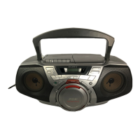
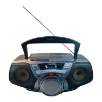
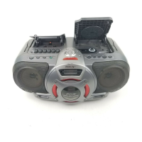
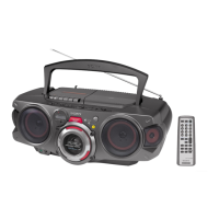
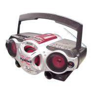
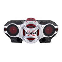
CFD-G35
Note on Schematic Diagram:
• All capacitors are in µF unless otherwise noted. p: pF.
50 WV or less are not indicated except for electrolytics
and tantalums.
• All resistors are in Ω and
1
/
4
W or less unless otherwise
specified.
•
f
: internal component.
• 2 : nonflammable resistor.
• C : panel designation.
• A : B+ Line.
• H : adjustment for repair.
•Total current is measured with no cassette installed.
•Power voltage is dc 9 V and fed with regulated dc power
supply from battery terminal.
•Voltages and waveforms are dc with respect to ground
under no-signal (detuned) conditions.
•Voltages are taken with a VOM (Input impedance 10 MΩ).
Voltage variations may be noted due to normal produc-
tion tolerances.
•Waveforms are taken with a oscilloscope.
Voltage variations may be noted due to normal produc-
tion tolerances.
• Circled numbers refer to waveforms.
• Signal path.
F : FM
f : AM
E : PB
a : REC
J : CD
•Abbreviation
AR : Argentina model.
AUS: Australian model.
CND : Canadian model.
E92 : Chilean and Peruvian model.
MX : Mexican model.
SP : Singapore model.
• WAVEFORMS
– TUNER Section –
SECTION 5
DIAGRAMS
5-1. Circuit Boards Location
BATT board
CD board
PDW boar
MAIN board
L-R/REG board
TC boardTRANS board
LCD board
BATT COM board
POWER board
TUNER board
HEADPHONE board
CONTROL (CD) board
CONTROL (POWER) board
CONTROL (VOL) board
Note on Printed Wiring Boards:
• X : parts extracted from the component side.
•
f
: internal component.
• : Pattern from the side which enables seeing.
(The other layers' patterns are not indicated.)
1
IC2 w; (XOUT)
1.4 Vp-p
13.3
µ
s
500 mV/DIV, 4
µ
s/DIV
– TC Section –
2
Q301 collector
(TAPE REC)
3.1 Vp-p
18
µ
s
1 V/DIV, 10
µ
s/DIV
– CD Section –
3
IC701 rk (XOUT)
4.2 Vp-p
59 ns
1 V/DIV, 20 ns/DIV
– MAIN Section –
4
IC801 ua (XT2)
3.6 Vp-p
30.5
µ
s
1 V/DIV, 10
µ
s/DIV
5
IC801 ug (X2)
3.7 Vp-p
238 ns
1 V/DIV, 100 ns/DIV
Ver 1.3 2002. 09
Note:
The components identified by
mark 0 or dotted line with mark
0 are critical for safety.
Replace only with part number
specified.
Note:
Les composants identifiés par
une marque 0 sont critiques
pour la sécurité.
Ne les remplacer que par une
pièce portant le numéro spécifié.
 Loading...