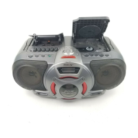
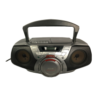
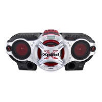
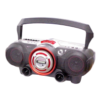
CFD-G550CP
21 21
CFD-G550CP
6-5. CIRCUIT BOARDS LOCATION6-3. NOTE FOR PRINTED WIRING BOARDS AND SCHEMATIC DIAGRAMS
THIS NOTE IS COMMON FOR PRINTED WIRING
BOARDS AND SCHEMATIC DIAGRAMS.
(In addition to this, the necessary note is
printed in each block.)
for schematic diagram:
• All capacitors are in µF unless otherwise noted. (p: pF)
50 WV or less are not indicated except for electrolytics
and tantalums.
• All resistors are in Ω and
1
/
4
W or less unless otherwise
specified.
•
f
: internal component.
• C : panel designation.
• A : B+ Line.
• H : adjustment for repair.
•Voltage and waveforms are dc with respect to ground
under no-signal conditions.
– CD/MP3 Board –
[]: CD PLAY
– TU Board –
no mark : FM
(): AM
– MAIN Board –
no mark : FM
<>: CD PLAY
– TC Board –
no mark : FM
(): PB
<>: REC
[]: CD PLAY
– Other Boards –
no mark : FM
•Voltages are taken with a VOM (Input impedance 10 MΩ).
Voltage variations may be noted due to normal produc-
tion tolerances.
•Waveforms are taken with a oscilloscope.
Voltage variations may be noted due to normal produc-
tion tolerances.
• Circled numbers refer to waveforms.
• Signal path.
F : FM
f : AM
J : CD PLAY
•Abbreviation
E41 : AC 230V are in E model.
MX : Mexican model.
for printed wiring boards:
• X : parts extracted from the component side.
• Y : parts extracted from the conductor side.
• W : indicates side identified with part number.
•
f
: internal component.
• : Pattern from the side which enables seeing.
(The other layer’s patterns are not indicated.)
C
B
These are omitted.
E
Q
B
These are omitted.
C
Q
Q
E
BCE
Note: The components identified by mark 0 or dotted line
with mark 0 are critical for safety.
Replace only with part number specified.
Caution:
Pattern face side: Parts on the pattern face side seen from
(Conductor Side) the pattern face are indicated.
Parts face side: Parts on the parts face side seen from
(Component Side) the parts face are indicated.
6-4. WAVEFORMS
BAT2 board
VOL board
POWER board
TRANS board
BAT1 board
LCD board
CONTROL 2 board
CONTROL 1 board
H/P board
TC board
TU board
MAIN board
CD/MP3 board
— TC BOARD —
1
Q301
C
(REC)
19.5µsec
2
T301, HRP301 (YEL)
4Vp-p
19.5µsec
40Vp-p
0.1V/div 5µsec/div
10V/div 5µsec/div
— CD/MP3 BOARD —
0.85±0.2Vp-p
1
IC701
4
(RF)
500mV/div 0.5µsec/div
2
IC701
qd
(FE)
100mV/div 200µsec/div
Approx. 100mVp-p
1.8V
3
IC701
qg
(TE)
100mV/div 200µsec/div
5
IC701
t;
(FSX/16MIN (I))
2V/div 50nsec/div
60nsec
IC1001
7
(CKIN (I))
2V/div 50nsec/div
4
IC701
rk
(XOUT)
2V/div 0.05µsec/div
6
Approx. 100mVp-p
1.8V
6Vp-p
16.9MHz
6Vp-p
60nsec
7Vp-p
— TU BOARD —
1
IC2
w;
(XOUT)
75kHz
1.5Vp-p
0.5V/div 5µsec/div
— MAIN BOARD —
1
IC801
ek
(X2)
4.2Vp-p
1V/div 0.2µsec/div
5MHz
 Loading...