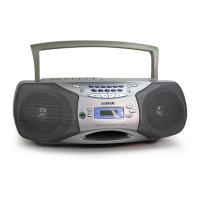
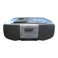
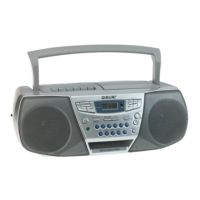
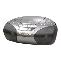
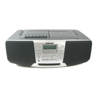
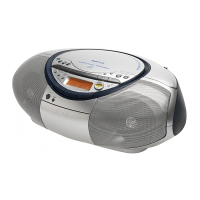
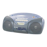
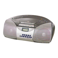
CFD-S400/S500
17 17
Pin No. Pin Name I/O Pin Description
75 X2 O Main system oscillation output (4.19 MHz)
76 RST I System reset input
77 V-CLK O Volume clock output
78 V-DATA O Volume data output
79 SCL O EEPROM clock output
80 SDA I/O EEPROM input/output
6-2. CIRCUIT BOARDS LOCATION
6-1. IC PIN DESCRIPTION
• IC802 uPD789477GC-A14-8BT (SYSTEM CONTROLLER)
Pin No. Pin Name I/O Pin Description
1, 2 NC — Not used. (Open)
3 to 5 VLC2 to 0 I LCD drive bias voltage output
6 to 9 COM0 to 3 O LCD drive common output
10 to 26 S0 to 16 O LCD drive segment output
27 REC I Tape record signal input H: REC
28 AC-CHK I AC power supply detection signal input L: AC in
29 CD-DOOR I CD door open/close switch input L: Close
30 S-ROCK O ROCK LED control signal output
31 S-POP O POP LED control signal output
32 S-JAZZ O JAZZ LED control signal output
33 S-VOCAL O VOCAL LED control signal output
34 S-SUR O SURROUND LED control signal output Not used. (Open)
35 A-MUTE O Audio mute output H: Mute
36 CD O CD function output H: CD
37 TAPE O Tape function output H: Tape
38 AVDD — Analog power supply pin for A/D converter (+3.3 V)
39 BTT-CHK-H I Battery check input for Hi-voltage
40 BTT-CHK-M I Battery check input for Mid-voltage
41 V-CHECK I Voltage transaction check input
42 to 45 KEY4 to 1 I Key input
46 MODE CHK I Destination setting input
47 AGND — Analog ground for A/D converter
48 REMOTE I Sircs receiver data input
49 TC-PLAY I Tape play switch input L: Play
50 WP/INI O Wake-up/Initial setting read signal output
51 MT-CONT O Motor control signal output Not used. (Open)
52 C-WRQ I CD write request data input
53 C-DOUT I CD digital signal processor data input
54 C-DIN O CD digital signal processor data output
55 C-CLK I CD serial data transfer clock signal input
56 R-COUNT I Tuner PLL IF count input
57 R-DATA O Tuner PLL data output
58 R-CLK O Tuner PLL clock output
59 R-LAT O Tuner PLL latch output
60 B-MUTE O Tuner mute signal output H: Mute
61 C-DRF I CD DRF signal input
62 C-CE O CD chip enable output
63 C-FSEQ I CD frame SYNC input
64 C-XRT O CD system reset output
65 P-CON O System power control output H: PCON
66 ISS1 O ISS1 output
67 ISS2 O ISS2 output
68 DBB O MEGA BASS control output H: MEGA BASS off, L: MEGA BASS on
69 ICO I Connected to VSS.
70 XT1 I Sub system oscillation input (32.768 kHz)
71 XT2 O Sub system oscillation output (32.768 kHz)
72 VDD — Main power supply pin for A/D converter (+3.3 V)
73 VSS — Main ground
74 X1 I Main system oscillation input (4.19 MHz)
SECTION 6
DIAGRAMS
 Loading...