4.19MHz
ESP : OFF
ESP : OFF
ESP : OFF
VOLT/DIV : 1 V AC
TIME/DIV : 0.1msec
VOLT/DIV : 1 V AC
TIME/DIV : 50µsec
VOLT/DIV : 1 V AC
TIME/DIV : 10msec
VOLT/DIV : 1 V AC
TIME/DIV : 0.2msec
VOLT/DIV : 1 V AC
TIME/DIV : 50nsec
VOLT/DIV : 1 V AC
TIME/DIV : 0.2msec
VOLT/DIV : 0.2 V AC
TIME/DIV : 0.5msec
r
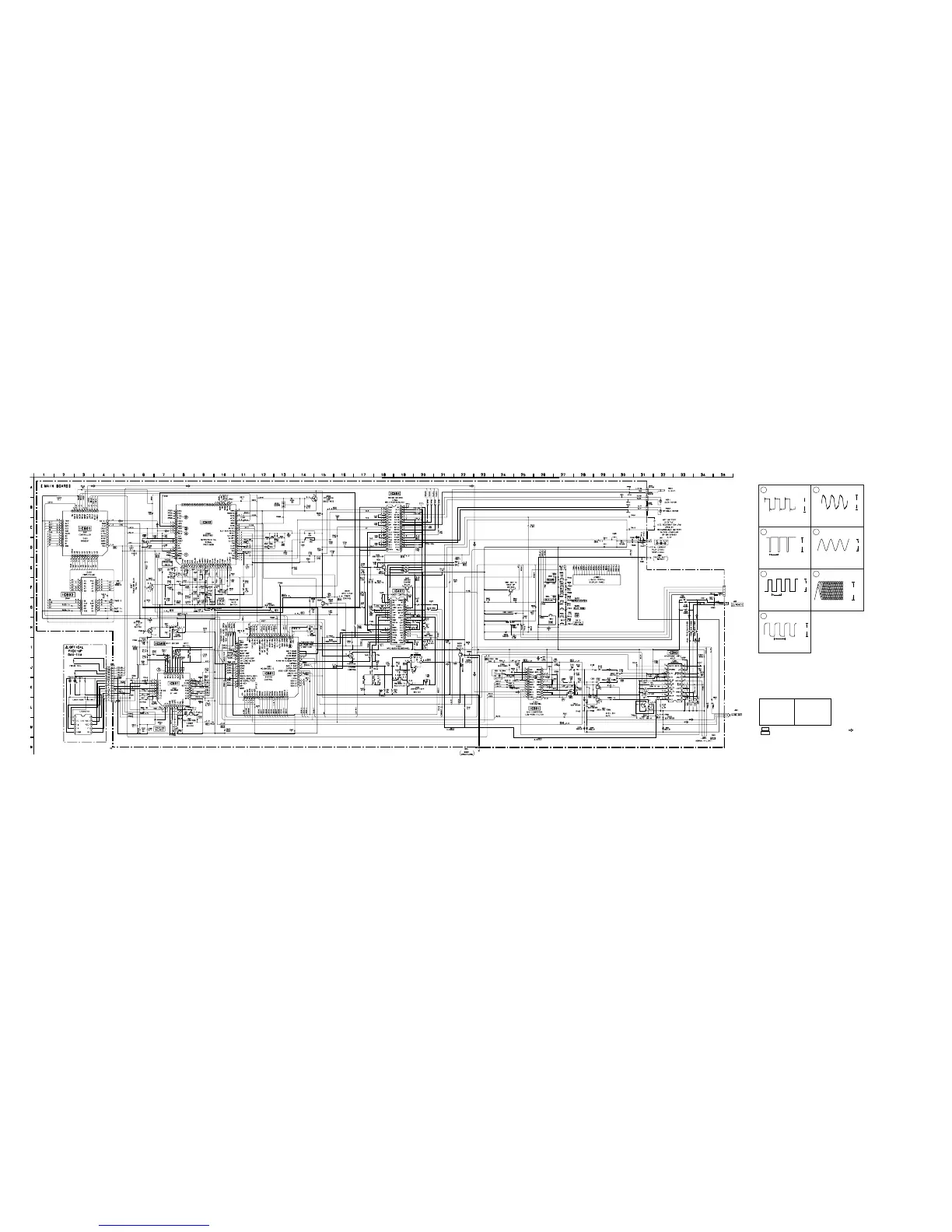
SCHEMATIC DIAGRAM
D-E300AN/E301/E305/E307CK/E307CKT
Note :
• All capacitors are in µF unless otherwise noted. pF: µµF
50WV or less are not indicated except for electrolytics and
tantalums.
• All resistors are in and
1
/
4
W or less unless otherwise
specified.
• ¢ : internal component.
Note :
The components identified
by mark ! or dotted line
with mark !are critical
for safety.
Replace only with part
number specified.
Note :
Les composants identifiés
par une marque !sont
critiques pour la sécurité.
Ne les remplacer que par
une pièce portant le numéro
spécifié.
•
B +
: B+ Line
•
: adjustment for repair.
• Power voltage is dc 4.5 V and fed with regulated dc power
supply from external power voltage jack (J401).
• Voltage and waveforms are dc with respect to ground under
no-signal conditions.
no mark : STOP
( ) : PLAY
• Voltages are taken with a VOM ( Input impedance 10M ).
Voltage variations may be noted due to normal production
tolerances.
• Waveforms are taken with a oscilloscope.
Voltage variations may be noted due to normal production
tolerances.
• Circled numbers refer to waveforms.
• Signal path.
: CD