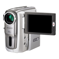
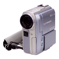
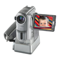
DCR-PC101/PC101EDCR-PC101/PC101E
COVER
COVER
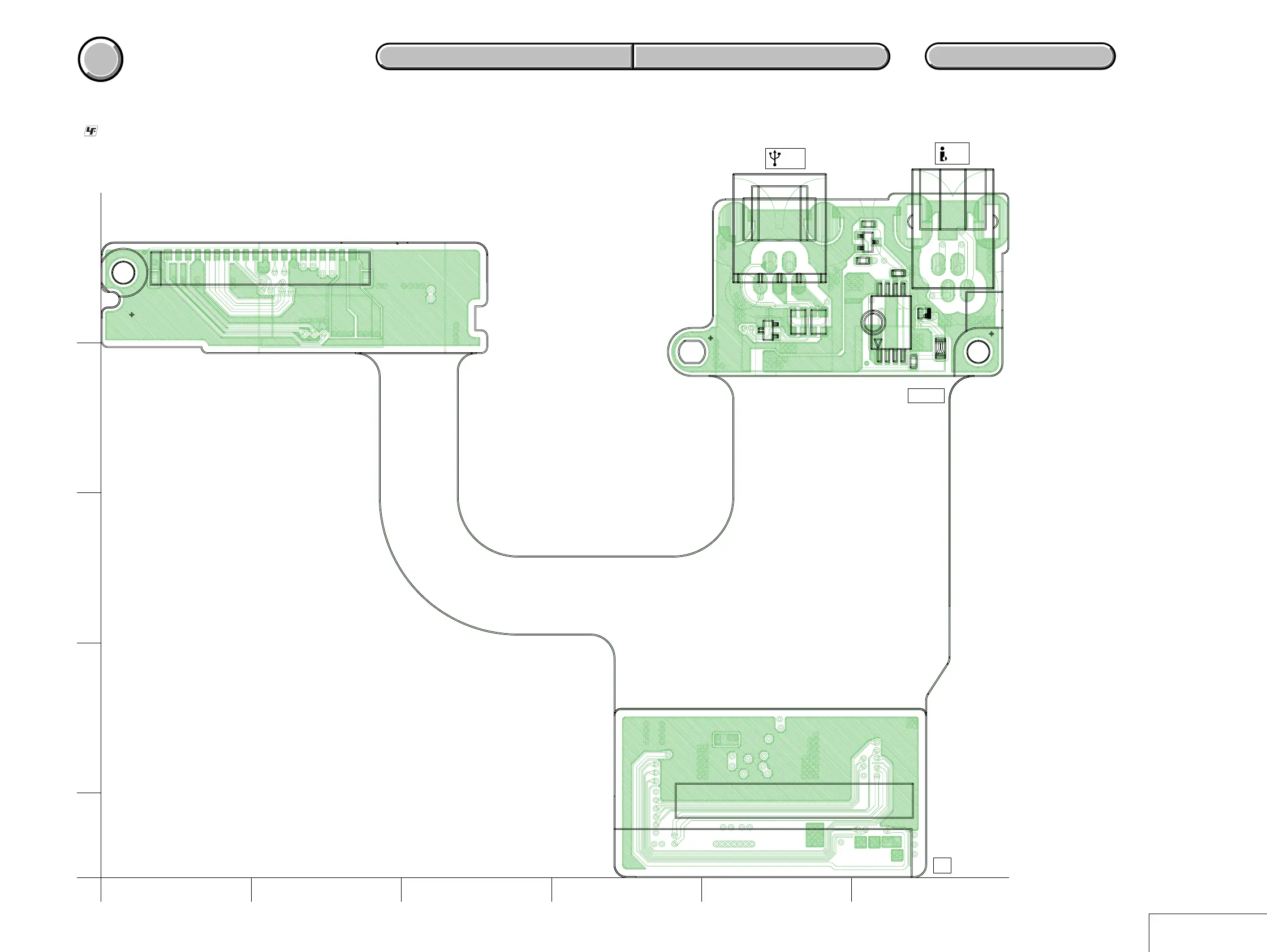
4-2. SCHEMATIC DIAGRAMS 4-3. PRINTED WIRING BOARDS
4-2. SCHEMATIC DIAGRAMS 4-3. PRINTED WIRING BOARDS
MOUNTED PARTS LOCATION
MOUNTED PARTS LOCATION
4-78
BJ-003 (SIDE A)
4-77
BJ-003 (DC IN, DV/USB CONNECTOR)
• For Printed Wiring Board.
• :Uses unleaded solder.
• BJ-003 board is six-layer print board. However, the patterns of
layers 2 to 5 have not been included in the diagram.
• There are a few cases that the part isn't mounted in this model
is printed on this diagram.
• See page 4-105 for printed parts location.
6
7
51
6
5
4
3
2
1
CN003
R004
R005
R013
LND001
LND002
LND003
D006
1
20
CN007
CN004
C001
LF001
1
23
Q001
Q005
D005
KA
LF002
4
58
1
Q002
BJ-003 BOARD(SIDE A)
B
A
C
D
1
2 3 4 5 6
E
1-684-899-
05
(USB)
(DV)
A
K
K
A
K
CHARGE
D005
11