THIS NOTE IS COMMON FOR PRINTED WIRING
BOARDS AND SCHEMATIC DIAGRAMS.
(In addition to this, the necessary note is printed
in each block.)
For schematic diagrams.
Note:
• All capacitors are in µF unless otherwise noted. pF: µµF
50 WV or less are not indicated except for electrolytics
and tantalums.
• All resistors are in Ω and
1
/
4
W or less unless otherwise
specified.
•
f
: internal component.
• C : panel designation.
For printed wiring boards.
Note:
• X : parts extracted from the component side.
•
a
: Through hole.
• b : Pattern from the side which enables seeing.
(The other layers' patterns are not indicated.)
• A : B+ Line.
• B : B– Line.
• H : adjustment for repair.
• Voltages and waveforms are dc with respect to ground
under no-signal (detuned) conditions.
• Voltages and waveforms are dc with respect to ground in
service mode.
• Waveforms are taken with a oscilloscope.
Voltage variations may be noted due to normal produc-
tion tolerances.
no mark : STOP
• Circled numbers refer to waveforms.
• Signal path.
F : FM
J : CD
c : DVD
g : VIDEO
G : Y
d : CHROMA
• Abbreviation
AR : Argentina model
AUS : Australian model
CND : Canadian model
EA : Saudi Arabia model
E12 : 220-240V AC area in E model
E32 : 110-240V AC area in E model
HK : Hong Kong model
KR : Korean model
MX : Mexican model
MY : Malaysia model
SP : Singapole model
TW : Taiwan model
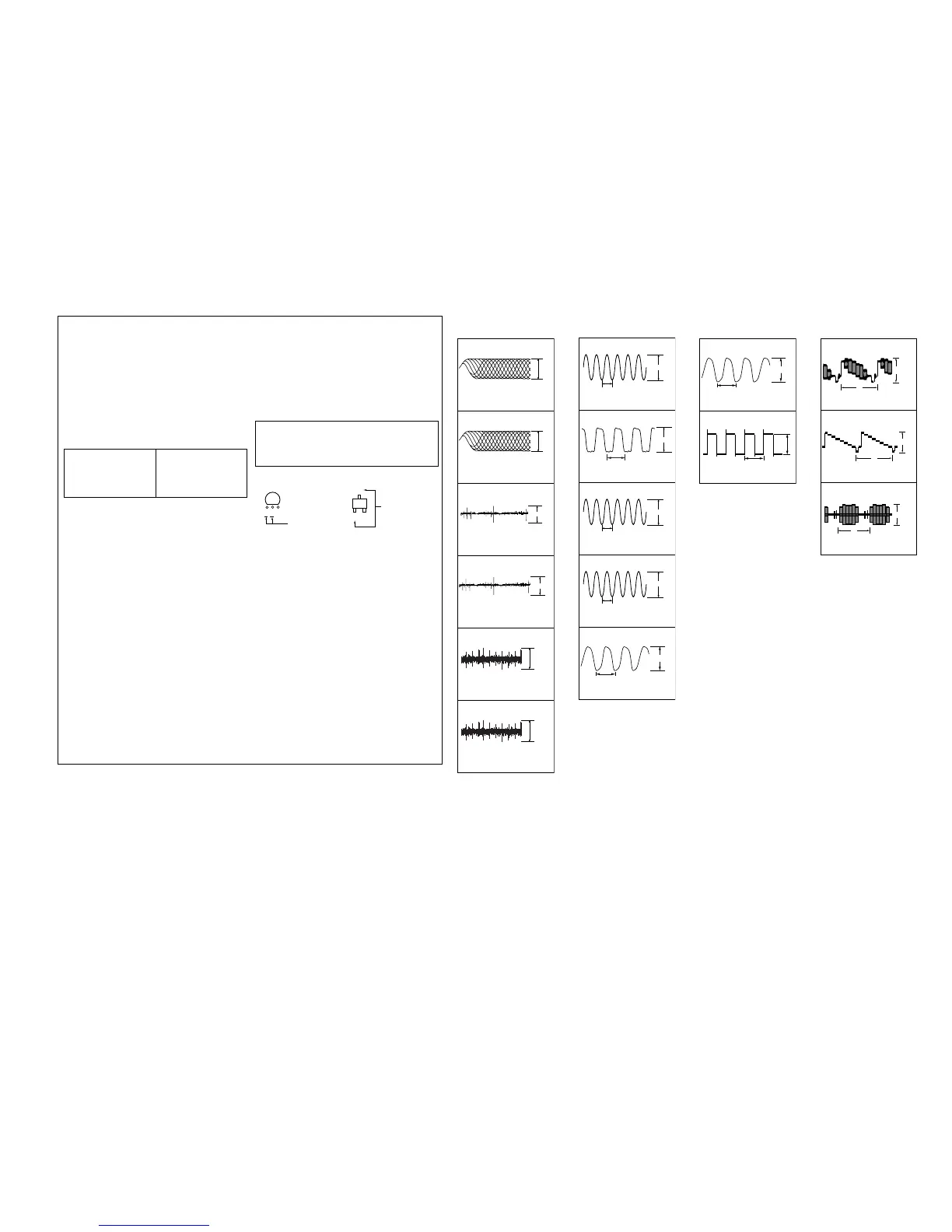
WAVEFORMS
– RF-240 BOARD –
1
2
3
4
5
6
1.5Vp-p
500mV/DIV 400ns/DIV
1.8Vp-p
500mV/DIV 40ms/DIV
1.8Vp-p
500mV/DIV 200ms/DIV
190mVp-p
100mV/DIV 40ms/DIV
840mVp-p
500mV/DIV 40ms/DIV
IC001 tl (SIGO) DVD PLAY
IC001 tl (SIGO) CD PLAY
IC001 ra (TE) DVD PLAY
IC001 ra (TE) CD PLAY
IC001 rs (FE) DVD PLAY
IC001 rs (FE) CD PLAY
1.5Vp-p
500mV/DIV 100ns/DIV
qs
qd
IC305 qd (OUTL1+)
7.2 Vp-p
5 Vp-p
13
µ
s
20.3ns (49.152MHz)
IC300 4
qf
qg
qh
IC701
qf
,
qg
Test Mode (Video)
IC701
9
,
0
Test Mode (Video)
Q700 E Test Mode (Video)
H
2.5Vp-p
H
0.9Vp-p
H
2Vp-p
– DVD BOARD –– AMP BOARD –– I/O BOARD –
Note:
The components identified by
mark ! or dotted line with mark
! are critical for safety.
Replace only with part number
specified.
Note:
Les composants identifiés par
une marque ! sont critiques
pour la sécurité.
Ne les remplacer que par une
pièce portant le numéro spécifié.
Caution:
Pattern face side: Parts on the pattern face side seen from
(Conductor B) the pattern face are indicated.
Parts face side: Parts on the parts face side seen from
(Component A) the parts face are indicated.