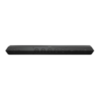
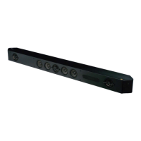
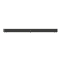
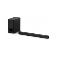
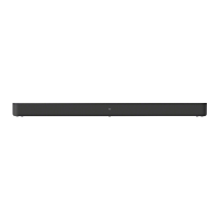
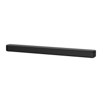
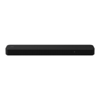
HT-ST5000
HT-ST5000
7979
THIS NOTE IS COMMON FOR PRINTED WIRING BOARDS AND SCHEMATIC DIAGRAMS.
(In addition to this, the necessary note is printed in each block.)
For Printed Wiring Boards.
Note:
• X : Parts extracted from the component side.
• Y : Parts extracted from the conductor side.
•
f
: Internal component.
• : Pattern from the side which enables seeing.
(The other layers’ patterns are not indicated.)
Caution:
Pattern face side:
(Conductor Side)
Parts face side:
(Component Side)
Parts on the pattern face side seen
from the pattern face are indicated.
Parts on the parts face side seen from
the parts face are indicated.
Caution:
Pattern face side:
(SIDE B)
Parts face side:
(SIDE A)
Parts on the pattern face side seen
from the pattern face are indicated.
Parts on the parts face side seen from
the parts face are indicated.
• AMP, AUDIO SELECTOR, BAR WIRED, DSP and MB-
1611 boards are multi-layer printed board. However, the
patterns of intermediate layers have not been included in
diagrams.
• Indication of transistor.
C
B
These are omitted.
E
Q
• Lead layouts
surface
CSP (Chip Size Package) Lead layout of conventional IC
For Schematic Diagrams.
Note:
• All capacitors are in μF unless otherwise noted. (p: pF)
50 WV or less are not indicated except for electrolytics
and tantalums.
• All resistors are in Ω and 1/4 W or less unless otherwise
specifi ed.
•
f
: Internal component.
• 2 : Nonfl ammable resistor.
• 5 : Fusible resistor.
• C : Panel designation.
Note:
The components identi-
fi ed by mark 0 or dotted
line with mark 0 are criti-
cal for safety.
Replace only with part
number specifi ed.
Note:
Les composants identifi és
par une marque 0 sont
critiques pour la sécurité.
Ne les remplacer que par
une pièce portant le nu-
méro spécifi é.
• A : B+ Line.
• Voltages and waveforms are dc with respect to ground
under no-signal conditions.
no mark
: POWER ON
*
: Impossible to measure
• Voltages are taken with VOM (Input impedance 10 M).
Voltage variations may be noted due to normal production
tolerances.
• Waveforms are taken with a oscilloscope.
Voltage variations may be noted due to normal production
tolerances.
• Circled numbers refer to waveforms.
• Signal path.
F : AUDIO
L : USB
a : WIRELESS LAN/Bluetooth
Note 1: When the complete AMP board is replaced, refer to
“SPREADING OF COMPOUND” on page 8.
Note 2: Among mounted electrical parts on each boards, only
parts that are described in the electrical parts list can
be replaced for repair.
The parts that are not described in the electrical parts
list cannot be replaced with single for repairing.
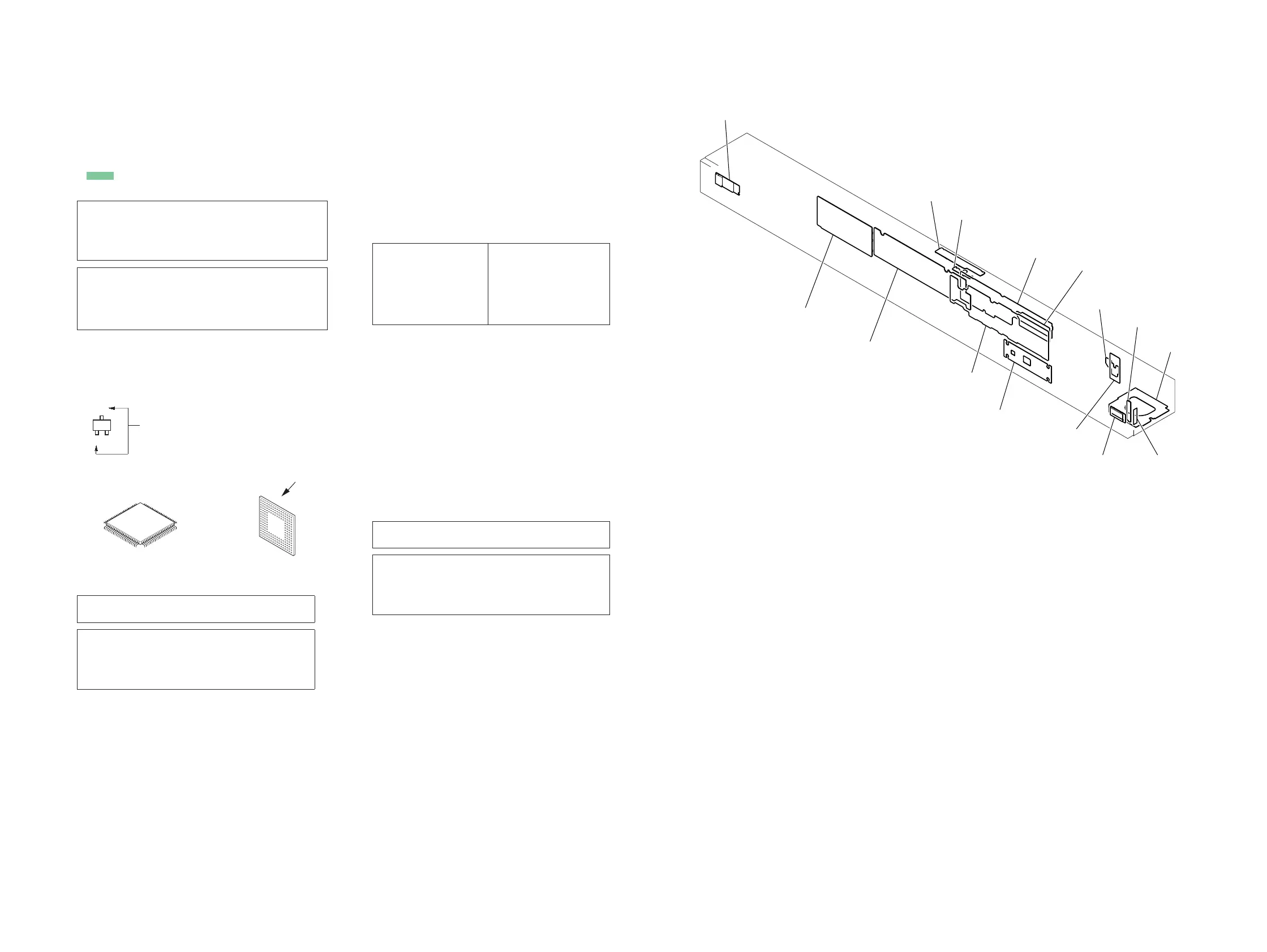
• Circuit Boards Location
KEY board
IR-REPEATER1 board
BAR POWER board
AUDIO SELECTOR board
DISPLAY board
DSP board
MB-1611 board
AMP board
BTW board
BAR WIRED board
CHUKEI-WIRE board
USB-CHUKEI board
NFC board
RF modulator
(RF1)
WLAN/BT combo card
(WIFI1)
 Loading...