2
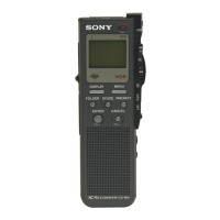
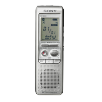
ICD-BM1/BM1A/BM1AVTP/BM1B/BM1DR9
TABLE OF CONTENTS
1. GENERAL
Index to Parts and Controls ............................................. 3
Using the Display Window .............................................. 3
Setting the Clock ............................................................. 3
2. DISASSEMBLY
2-1. Knob (Rear) ..................................................................... 4
2-2. Chassis Block Assy ......................................................... 5
2-3. SW Board ........................................................................ 5
2-4. Plate (MS) Section........................................................... 6
2-5. LCD Board ...................................................................... 6
2-6. Chassis Section ................................................................ 7
2-7. Memory Stick Connector ................................................ 7
2-8. Main Board ...................................................................... 8
3. DIAGRAMS
3-1. Block Diagram – Main Section – .................................... 9
3-2. Block Diagram – LCD/SW Section – ............................. 10
3-3. Printed Wiring Board – Main Section – .......................... 12
3-4. Schematic Diagram – Main Section (1/3) – .................... 13
3-5. Schematic Diagram – Main Section (2/3) – .................... 14
3-6. Schematic Diagram – Main Section (3/3) – .................... 15
3-7. Schematic Diagram – LCD/SW Section – ...................... 16
3-8. Printed Wiring Board – LCD Section– ............................ 17
3-9. Printed Wiring Board – SW Section– .............................. 18
4. EXPLODED VIEWS
4-1. Main Section .................................................................... 27
4-2. Case Section .................................................................... 28
4-3. Ornament Section ............................................................ 29
4-4. Chassis (1) Section .......................................................... 30
4-5. Chassis (2) Section .......................................................... 31
5. ELECTRICAL PARTS LIST .................................. 32
Flexible Circuit Board Repairing
• Keep the temperature of the soldering iron around 270 ˚C
during repairing.
• Do not touch the soldering iron on the same conductor of the
circuit board (within 3 times).
• Be careful not to apply force on the conductor when soldering
or unsoldering.
Notes on chip component replacement
• Never reuse a disconnected chip component.
• Notice that the minus side of a tantalum capacitor may be
damaged by heat.
* Replacement of IC601, IC702 used in this set requires a special
tool.
•The voltage and waveform of CSP (chip size package) cannot
be measured, because its lead layout is different from that of
conventional IC.
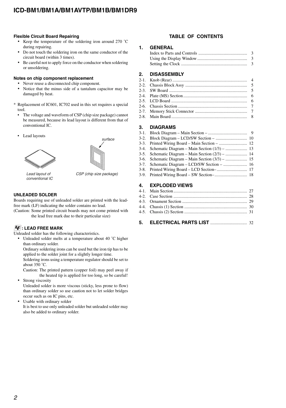
• Lead layouts
Lead layout of
conventional IC
CSP (chip size package
surface
UNLEADED SOLDER
Boards requiring use of unleaded solder are printed with the lead-
free mark (LF) indicating the solder contains no lead.
(Caution: Some printed circuit boards may not come printed with
the lead free mark due to their particular size)
: LEAD FREE MARK
Unleaded solder has the following characteristics.
• Unleaded solder melts at a temperature about 40 ˚C higher
than ordinary solder.
Ordinary soldering irons can be used but the iron tip has to be
applied to the solder joint for a slightly longer time.
Soldering irons using a temperature regulator should be set to
about 350 ˚C.
Caution: The printed pattern (copper foil) may peel away if
the heated tip is applied for too long, so be careful!
• Strong viscosity
Unleaded solder is more viscous (sticky, less prone to flow)
than ordinary solder so use caution not to let solder bridges
occur such as on IC pins, etc.
• Usable with ordinary solder
It is best to use only unleaded solder but unleaded solder may
also be added to ordinary solder.
 Loading...