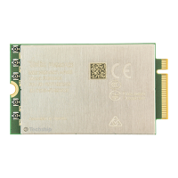
FN990 Family Hardware Design Guide
the Add-in Card, being tied to GND or left No Connect (NC), the detected pins will
create a 4-bit logic state that requires decoding.
Used by an Add-in Card where USB 3.1 Gen1 is present on the connector and PCIe
is No Connect.
Only a single lane of PCIe is available in these configurations.
For more details, please refer to the PCI Express M.2 Specification document.
3.5 Block Diagram
The figure below shows an overview of the internal architecture of the FN990 Family
module.
Figure 1: FN990 Family Block Diagram
3.6 RF Performance
The RF performance in 5G, LTE, and WCDMA modes conforms to the 3GPP specifications.
Conducted Transmit Output Power
TX power follows the measurement conditions and specifications defined in 3GPP.
Table 7: Conducted Transmit Output Power
5G NR Sub-6
n1, n2, n3, n5, n7, n8, n12, n13, n14, n18, n20, n25, n26, n28,
n30, n38, n40, n41, n48**, n66, n71, n77, n78, n79
5G NR Sub-6 n41, n77, n78, n79
Supports Power Class 2
 Loading...