Performance Considerations
4-61PipelineSPRU733
Depending on the type of memory and the time required to complete an
access, the pipeline may stall to ensure proper coordination of data and
instructions. This is discussed in section 4.4.3.1.
In the instance where multiple accesses are made to a single ported memory,
the pipeline will stall to allow the extra access to occur. This is called a memory
bank hit and is discussed in section 4.4.3.2.
4.4.3.1 Memory Stalls
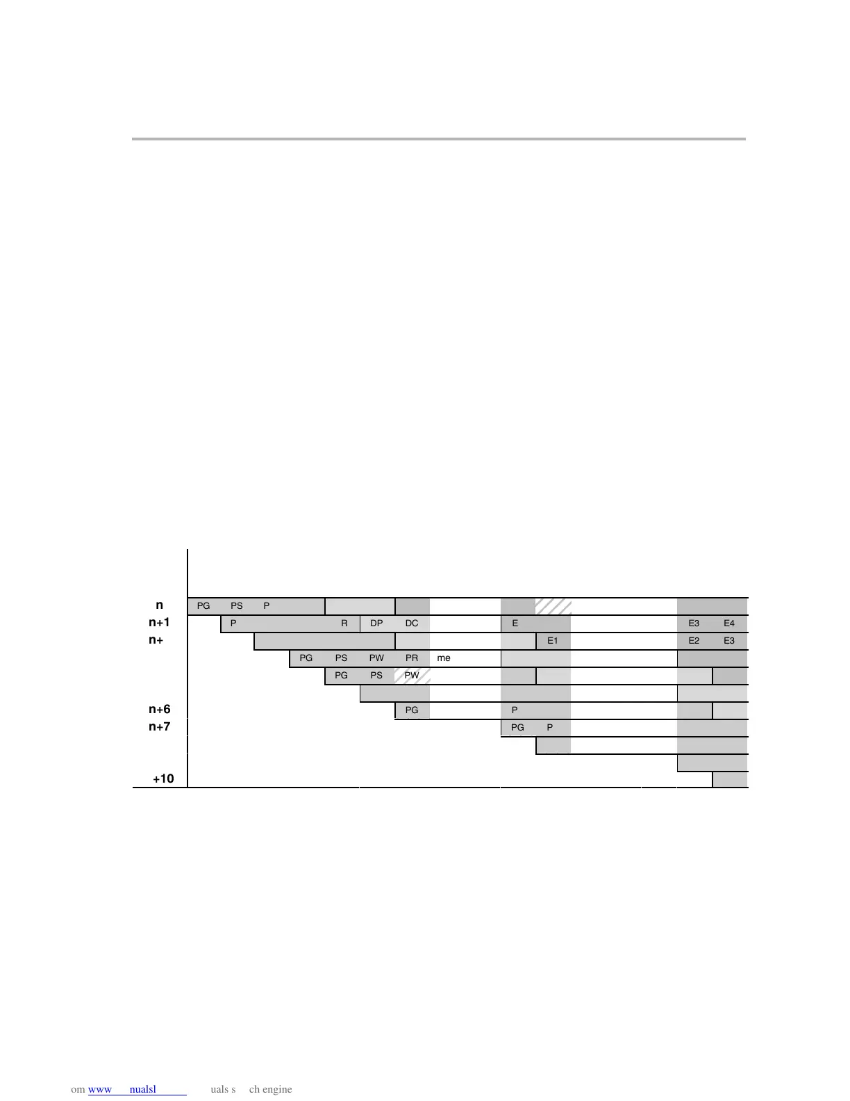
A memory stall occurs when memory is not ready to respond to an access from
the CPU. This access occurs during the PW phase for a program memory
access and during the E3 phase for a data memory access. The memory stall
causes all of the pipeline phases to lengthen beyond a single clock cycle,
causing execution to take additional clock cycles to finish. The results of the
program execution are identical whether a stall occurs or not. Figure 4−32
illustrates this point.
Figure 4−32. Program and Data Memory Stalls
Clock cycle
Fetch
packet
(FP)
1
2345678910111213141516



 To Next Page