MT8206
PRELIMINARY, SUBJECT TO CHANGE WITHOUT NOTICE MTK CONFIDENTIAL, NO DISCLOSURE
June, 2006
10.2
DC CHARACTERISTICS MEASUREMENT VALUE
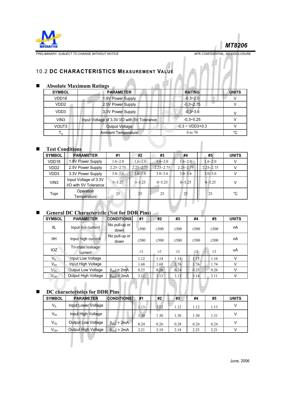
Absolute Maximum Ratings
SYMBOL PARAMETER RATING UNITS
VDD18 1.8V Power Supply
-0.3~2.0
V
VDD2 2.5V Power Supply
-0.3~2.75
V
VDD3 3.3V Power Supply
-0.3~3.6
V
VIN3 Input Voltage of 3.3V I/O with 5V Tolerance
-0.3~5.25 V
VOUT3 Output Voltage
-0.3 ~ VDD3+0.3 V
T
a
Ambient Temperature
0 to 70
°C
Test Conditions
SYMBOL PARAMETER #1 #2 #3 #4 #5 UNITS
VDD18
1.8V Power Supply
1.6~2.0 1.6~2.0 1.6~2.0 1.6~2.0 1.6~2.0
V
VDD2
2.5V Power Supply
2.25~2.75 2.25~2.75 2.25~2.75 2.25~2.75 2.25~2.75
V
VDD3
3.3V Power Supply
3.0~3.6 3.0~3.6 3.0~3.6 3.0~3.6 3.0~3.6
V
VIN3
Input Voltage of 3.3V
I/O with 5V Tolerance
0~5.25 0~5.25 0~5.25 0~5.25 0~5.25
V
Topr
Operation
Temperature
25 25 25 25 25 °C
General DC Characteristic (Not for DDR Pins)
SYMBOL PARAMETER CONDITIONS #1 #2 #3 #4 #5 UNITS
IIL Input low current
No pull-up or
down
d500 d500 d500 d500 d500
nA
IIH Input high current
No pull-up or
down
d500 d500 d500 d500 d500
nA
IOZ
Tri-state leakage
current
d1 d1 d1 d1 d1
uA
V
IL
Input Low Voltage
1.12 1.14 1.14 1.15 1.16 V
V
IH
Input High Voltage
1.68 1.69 1.76 1.76 1.74 V
V
OL
Output Low Voltage
|I
OL
| = 2mA 0.25 0.26 0.24 0.25 0.26 V
V
OH
Output High Voltage
|I
OH
| = 2mA 3.12 3.13 3.13 3.14 3.11 V
DC characteristics for DDR Pins
SYMBOL PARAMETER CONDITIONS #1 #2 #3 #4 #5 UNITS
V
IL
Input Lower Voltage
1.13 1.12 1.12 1.12 1.13
V
V
IH
Input High Voltage
1.30 1.30 1.30 1.30 1.31
V
V
OL
Output Low Voltage
|I
OL
| = 2mA
0.24 0.26 0.28 0.24 0.24
V
V
OH
Output High Voltage
|I
OH
| = 2mA 2.21 2.19 2.18 2.23 2.21 V