e-STUDIO555/655/755/855 © 2009 - 2011 TOSHIBA TEC CORPORATION All rights reserved
COPY PROCESS
3 - 2
3.2 Details of Copy Process
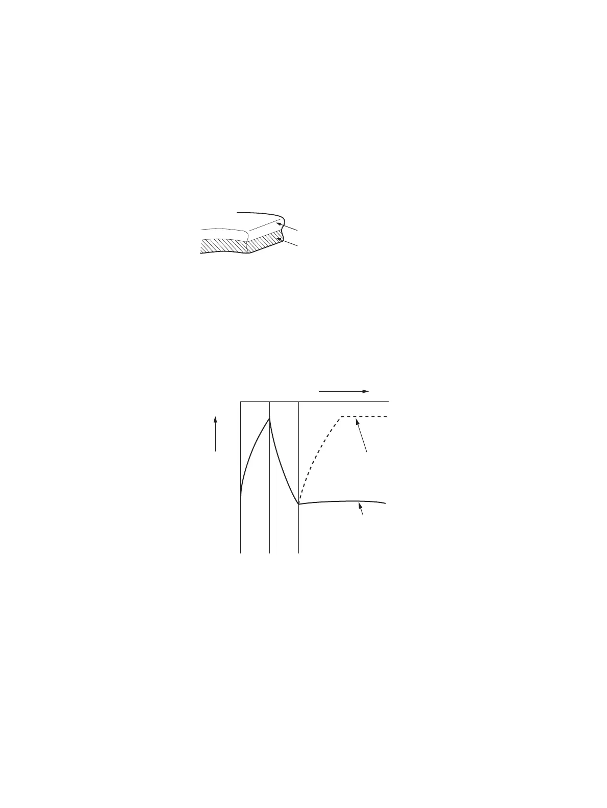
(1) Photoconductive drum
The photoconductive drum consists of two layers, an outer and an inner layer. The outer layer is a
photoconductive layer made of an organic photoconductive carrier (OPC).
The inner layer is an aluminum conductive base in a cylindrical form.
The photoconductive carrier has the characteristic that its electrical resistance changes depending
on the strength of the light exposed.
Example:
• Strong light
Resistance is decreased (works as a conductor.)
• Weak light
Resistance is increased (works as an insulator.)
Fig. 3-2
[Formation of electrostatic latent image]
In the processes of charging, scanning, printing and discharging described later, negative potential
on the areas of the drum corresponding to black areas of the original is eliminated, while the areas
of the drum corresponding to white areas remains the negative charge.
As this image on the drum formed by the negative potential is invisible, it is called an “electrostatic
latent image’’.
Fig. 3-3
Photoconductive layer
Aluminum conductive base
Structure of the photoconductive drum (OPC)
0
Time
(
t
)
Black area of original
White area of original
Electric potential on the photoconductive drum
Surface potential
(
V
)
Discharge
process
Charging
process
-300
-600
 Loading...