NINA-B4 series - System integration manual
UBX-19052230 - R06 Functional description Page 7 of 45
C1-Public
1.3 Block diagrams
Block diagrams of the NINA-B40 and NINA-B41 module designs are shown in Figure 1 and Figure 2.
1.3.1 NINA-B40
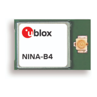
A block diagram of the NINA-B40 open-cpu module design showing the alternative U.FL connector
(B400), antenna pin (B401), and PCB trace antenna (B406) solutions is shown in Figure 1.
☞ NINA-B400 modules include a U.FL connector for connecting an external antenna. The module size
is 10 x 15 x 2.2 mm.
☞ NINA-B401 modules include an ANT pad on the footprint for connecting an external antenna. The
module size is 10 x 11.6 x 2.2 mm.
☞ NINA-B406 module support an internal PCB trace antenna using antenna technology from Proant
AB. The module size is 10 x 15 x 2.2 mm.
Figure 1: NINA-B40 series block diagram
DC/DC and LDO regulators
512 kB flash
Bluetooth LE
baseband
IO buffers
Arm® Cortex®-M4
with FPU
PLL
– 3.6 V)
– 3.6 V)
32 MHz
SPI
1.3 V
System
power
ADC and
Analog
Passive NFC tag
128 kB
RAM
PLL
RTC, timers
and counters
RF
Nordic Semiconductor
USB device
(NINA-B406)
PCB trace antenna
(NINA-B400)
U.FL antenna connector
(NINA-B401)
Antenna pin
 Loading...