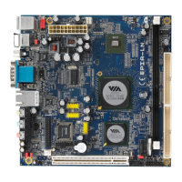
BIOS Setup
3-25
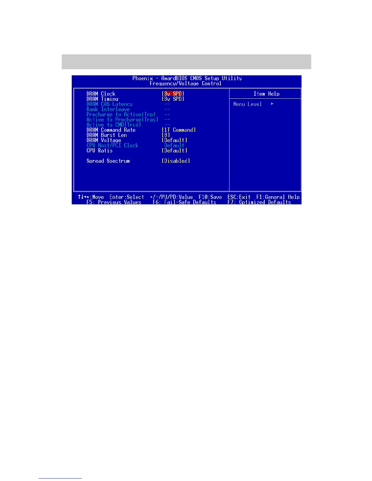
Frequency/Voltage Control
DRAM Clock
The chipset supports synchronous and asynchronous mode between host clock
and DRAM clock frequency. Settings: By SPD, 100MHz and 133MHz.
DRAM Timing
This setting determines whether DRAM timing is configured by reading the
contents of the SPD (Serial Presence Detect) EPROM on the DRAM module.
Selecting Yes makes SDRAM Cycle Length and Bank Interleave automatically
determined by BIOS according to the configurations on the SPD. Settings: Manual
and By SPD.
SDRAM CAS Latency
Set the time between SDRAM read command and when the data actually be-
comes available. Settings: 2 and 2.5.
Bank Interleave
Set the interleave mode of the SDRAM interface. Interleaving allows banks of
SDRAM to alternate their refresh and access cycles. One bank will undergo its
refresh cycle while another is being accessed. This improves performance of the
SDRAM by masking the refresh time of each bank. Settings: Disabled, 2 Bank
and 4 Bank.
Precharge to Active (Trp)
Set the time from DRAM precharge to active state. Settings: 2T and 3T.
 Loading...