(4)
Digital Switch
When the
digital
switch is selected
by the
dial/digital
switch selector
(2)
the index
(^)
lights
and
the frequency
output is
determined
by the digital
switch and
the
FREQ
MULT.
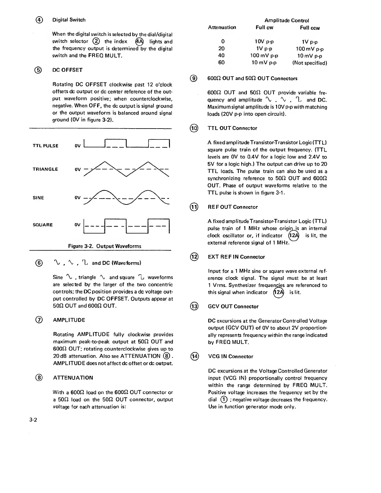
(5)
DC
OFFSET
Rotating DC
OFFSET
clockwise past 12
o'clock
offsets dc output
or dc center reference
of the out-
put
waveform
positive;
when counterclockwise,
negative. When
OFF,
the
dc output is
signal
ground
or the output
waveform is
balanced around signal
ground (OV in
figure 3-2).
TTL
PULSE
TRIANGLE
SINE
SQUARE
Figure
3-2.
Output Waveforms
(6)
\
,
\
,
n_i
and
DC
(Waveforms)
Sine
\
,
triangle
\
and square
r
L
waveforms
are selected by the larger
of the two concentric
controls; the Deposition provides
a dc
voltage
out-
put
controlled
by DC OFFSET.
Outputs
appear
at
500 OUT and
6000 OUT.
(
J
)
AMPLITUDE
Rotating
AMPLITUDE
fully
clockwise
provides
maximum peak-to-peak
output at
500
OUT and
6000 OUT; rotating
counterclockwise gives up to
20 dB
attenuation. Also
see ATTENUATION
(§)
.
AMPLITUDE does not affect dc offset or dc output.
(8)
ATTENUATION
With
a
6000 load on the
6000 OUT connector or
a 500 load on the 500 OUT
connector, output
voltage
for
each
attenuation
is:
Amplitude
Control
Attenuation
Full
cw
Full
ccw
0 10V
p-p
IV
p-p
20 IV
p-p 100 mV
p-p
40 100
mV
p-p
10 mV
p-p
60 10 mV
p-p
(Not
specified)
©
6000
OUT and 500
OUT Connectors
6000 OUT
and
500 OUT provide
variable
fre-
quency
and amplitude
%
,
\
,
T,
and
DC.
Maximumsignal amplitude is 10V
p-p
with
matching
loads
(20V
p-p
into open circuit).
@
TTL OUT Connector
A fixed ampl itude T
ransistor-T ransistor
Logic <TT
L)
square pulse train
of
the output
frequency.
(TTL
levels are OV to 0.4V
for
a
logic low
and 2.4V
to
5V for a
logic high.)
The output
can drive
up to 20
TTL loads.
The pulse train can also
be
used
as
a
synchronizing reference
to
50f2 OUT and
6000
OUT.
Phase of
output
waveforms relative
to the
TTL pulse
is shown
in
figure
3-1.
(11)
REF
OUT Connector
A fixed
amplitudeTransistor-Transistor
Logic
(TTL)
pulse
train
of
1 MHz
whose
originjs an
internal
clock oscillator or, if indicator
fl2A
is lit,
the
external reference signal of 1
MHz.
(12)
EXT RE F IN Connector
Input
for
a
1
MHz
sine or square
wave external ref-
erence clock signal. The signal must be at least
1 Vrms. Synthesizer
frequencies
are referenced
to
this signal when indicator
H2A
is lit.
(j3)
GCV
OUT Connector
DC excursions
at
the Generator Controlled Voltage
output (GCV
OUT)
of OV
to
about 2
V
proportion-
ally represents
frequency within
the range indicated
by
FREQ
MULT.
(14)
VCG
IN Connector
DC excursions
at
the Voltage Controlled Generator
input (VCG IN) proportionally control
frequency
within
the range determined
by
FREQ MULT.
Positive
voltage increases the frequency set by
the
dial
(T)
;
negative
voltage decreases
the frequency.
Use
in
function generator
mode
only.
3-2
 Loading...