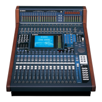
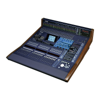
DM2000
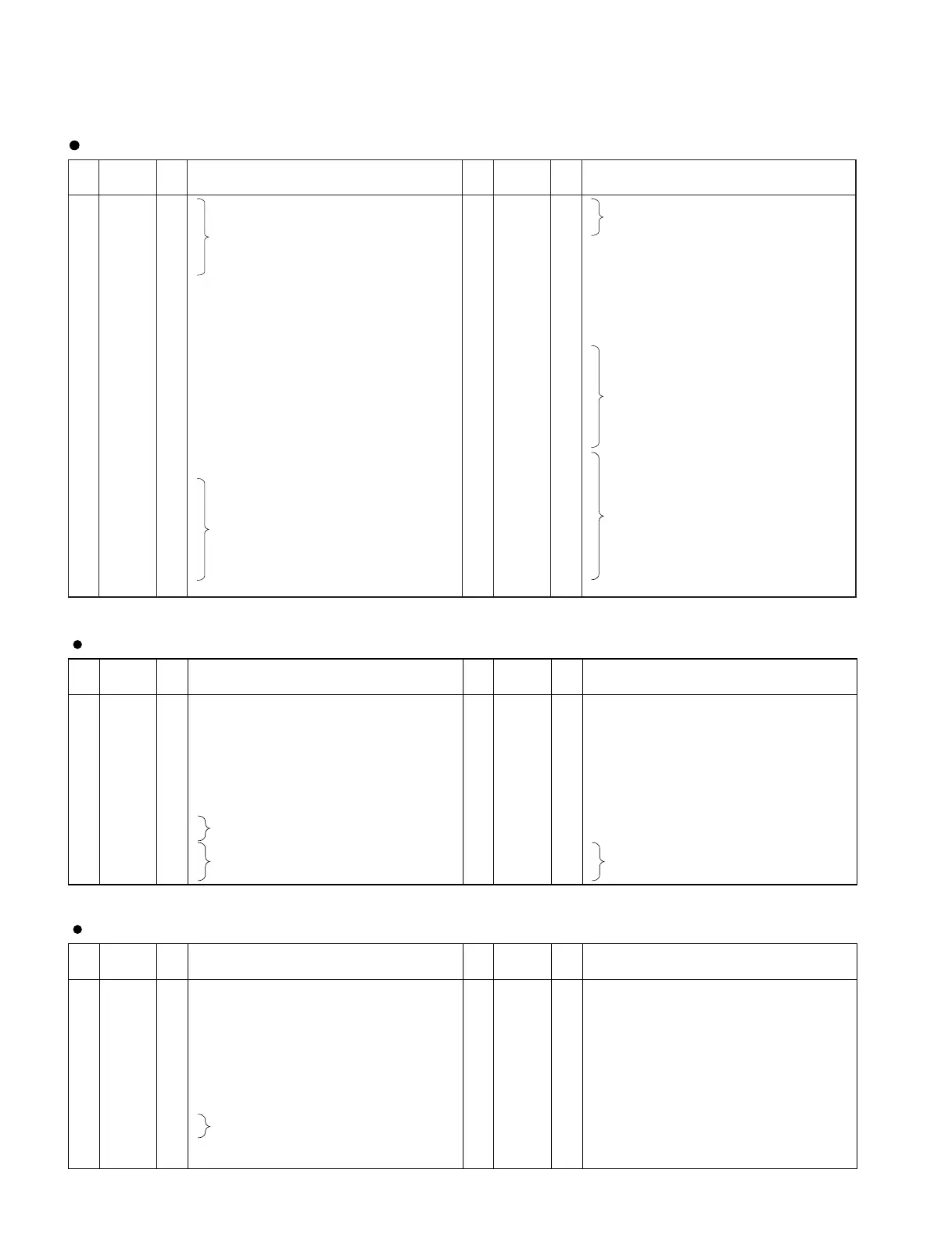
68
PIN
NO.
1
2
3
4
5
6
7
8
9
10
11
12
13
14
15
16
17
18
19
20
21
22
23
24
25
26
27
28
29
30
I/O
O
O
O
O
O
O
O
O
-
I
-
-
I
I
I
I
I
O
I
I
-
I/O
I/O
I/O
I/O
I/O
I/O
I/O
I/O
O
VA5
VA4
VA3
VA2
VA1
VA0
/VWR
/VCE
/VRD
/RES
NC
NC
/RD
/WR
SEL2
SEL1
OSC1
OSC2
/CS
A0
Vdd
D0
D1
D2
D3
D4
D5
D6
D7
XD3
NAME
VRAM address bus
VRAM read/write
Memory control
Not used
Initial clear
Not used
Not used
Read strobe
Write strobe
Bus select
Bus select
Clock
Clock
Chip select
Data mode select
Power supply
Data bus
Data bus output for 4 bit dot
FUNCTION
PIN
NO.
31
32
33
34
35
36
37
38
39
40
41
42
43
44
45
46
47
48
49
50
51
52
53
54
55
56
57
58
59
60
I/O
O
O
O
O
O
-
O
O
O
O
O
I/O
I/O
I/O
I/O
I/O
I/O
I/O
I/O
O
O
O
O
O
O
O
O
O
O
-
XD2
XD1
XD0
XECL
XSCL
Vss
LP
WF
YDIS
YD
YSCL
VD7
VD6
VD5
VD4
VD3
VD2
VD1
VD0
VA15
VA14
VA13
VA12
VA11
VA10
VA9
VA8
VA7
VA6
NC
NAME
Data bus output for 4 bit dot
S driver enable, chain clock
Data bus shift clock
Ground
X driver latch pulse
Frame signal for X/Y driver
Power down signal for displaying off mode
Scan start signal
Scan shift clock
VRAM data bus
VRAM address bus
Not used
FUNCTION
S1D13305F00B100 (XQ595A00) LCDC (LCD Controller)
CPU: IC129
PIN
NO.
I/O FUNCTIONNAME
PIN
NO.
I/O FUNCTIONNAME
1
2
3
4
5
6
7
8
9
10
11
12
13
14
DVSS
DVDD
MCLK
/PD
BICK
SDATA
LRCK
SMUTE//CS
DFS
DEM0/CCLK
DEM1/CDTI
DIF0
DIF1
DIF2
-
-
I
I
I
I
I
I
I
I
I
I
I
I
Digital ground
Digital power supply
Master clock
Power down mode
Audio serial data clock
Audio serial data input
L/R clock
Soft mute
Double speed sampling mode
De-emphasis enable
Digital input format
15
16
17
18
19
20
21
22
23
24
25
26
27
28
BVSS
VREFL
VREFH
AVDD
AVSS
AOUTR-
AOUTR+
AOUTL-
AOUTL+
VCOM
P//S
CKS0
CKS1
CKS2
-
I
I
-
-
O
O
O
O
O
I
I
I
I
Substrate ground
Low level voltage reference
High level voltage reference
Analog power supply +5 V
Analog ground
Rch negative analog output
Rch positive analog output
Lch negative analog output
Lch positive analog output
Common voltage output
Parallel/serial select
Master clock select
AK4393-VF-E2 (XW029A00) DAC (Digital to Analog Converter)
DA2: IC903-906
DA1: IC903-906
PIN
NO.
I/O FUNCTIONNAME
PIN
NO.
I/O FUNCTIONNAME
1
2
3
4
5
6
7
8
9
10
11
12
13
14
VREFL
GNDL
VCOML
AINL+
AINL-
ZCAL
VD
DGND
CAL
/RST
SMODE2
SMODE1
LRCK
SCLK
O
O
I
I
I
O
I
I
I
I/O
I/O
Lch voltage reference output
Lch ground
Lch common voltage
Lch positive analog input
Lch negative analog input
Zero calibration
Digital power supply +3.3V
Digital ground
Calibration status
Reset
Serial interface mode select
L/R channel select clock
Serial data clock
15
16
17
18
19
20
21
22
23
24
25
26
27
28
SDATA
FSYNC
MCLK
DFS
HPFE
TEST
BGND
AGND
VA
AINR-
AINR+
VCOMR
GNDR
VREFR
O
I/O
I
I
I
I
I
I
O
O
Serial data output
Frame synchronization clock
Master clock input
Double speed sampling mode select
HPF enable
Test
Substrate ground
Analog ground
Analog power supply +5V
Rch negative analog input
Rch positive analog input
Rch common voltage
Rch ground
Rch voltage reference output
AK5393-VS-E2 (XZ298A00) ADC (Analog to Digital Converter)
AD: IC103, 203, 303, 403, 503, 603
DA2: IC951-953
 Loading...