Hardware and physical integration guideline A1 PCR sensors
Page 11 of 30
2024-02-07 © 2024 by Acconeer – All rights reserved
inside the footprint has lower impact on the radiated performance and therefore some vias and short
traces are preferably placed there while still satisfying regulatory compliance.
- Minimize copper clearance for traces, vias and pads on the sensor layer.
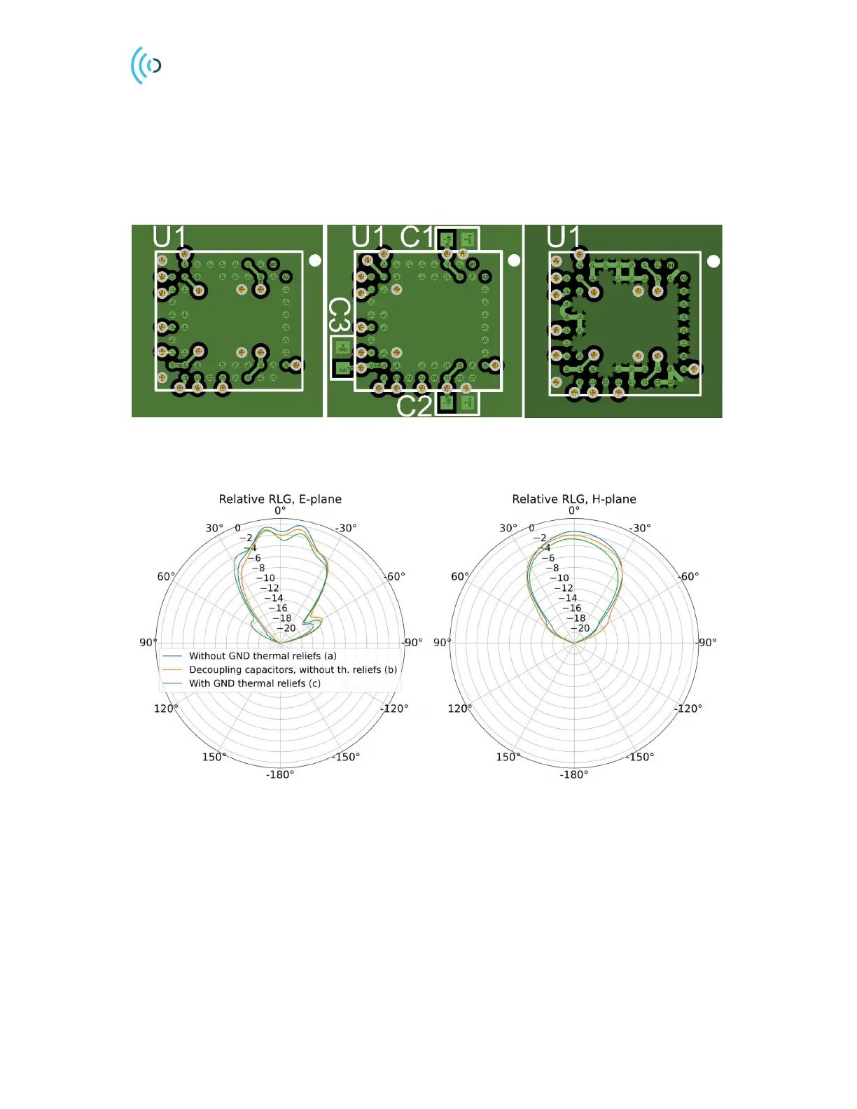
- If the PCB assembly process allows, connect all ground pads without thermal reliefs as shown in
Figure 6a-b. This can increase the boresight RLG by approximately 1.5 dB compared to Figure 6c,
provided there are no other interfering components or PCB traces close to the sensor, see Figure 7.
Figure 6. A111 routing examples with vias placed close to sensor for maximizing ground plane size. (a) Without GND
thermal reliefs, (b) with decoupling capacitors and without GND thermal reliefs, (c) with GND thermal reliefs. Trace
to copper clearance is 0.127 mm.
Figure 7. Relative RLG loss with and without A111 thermal reliefs.
 Loading...