Hardware and physical integration guideline A1 PCR sensors
Page 10 of 30
© 2024 by Acconeer – All rights reserved 2024-02-07
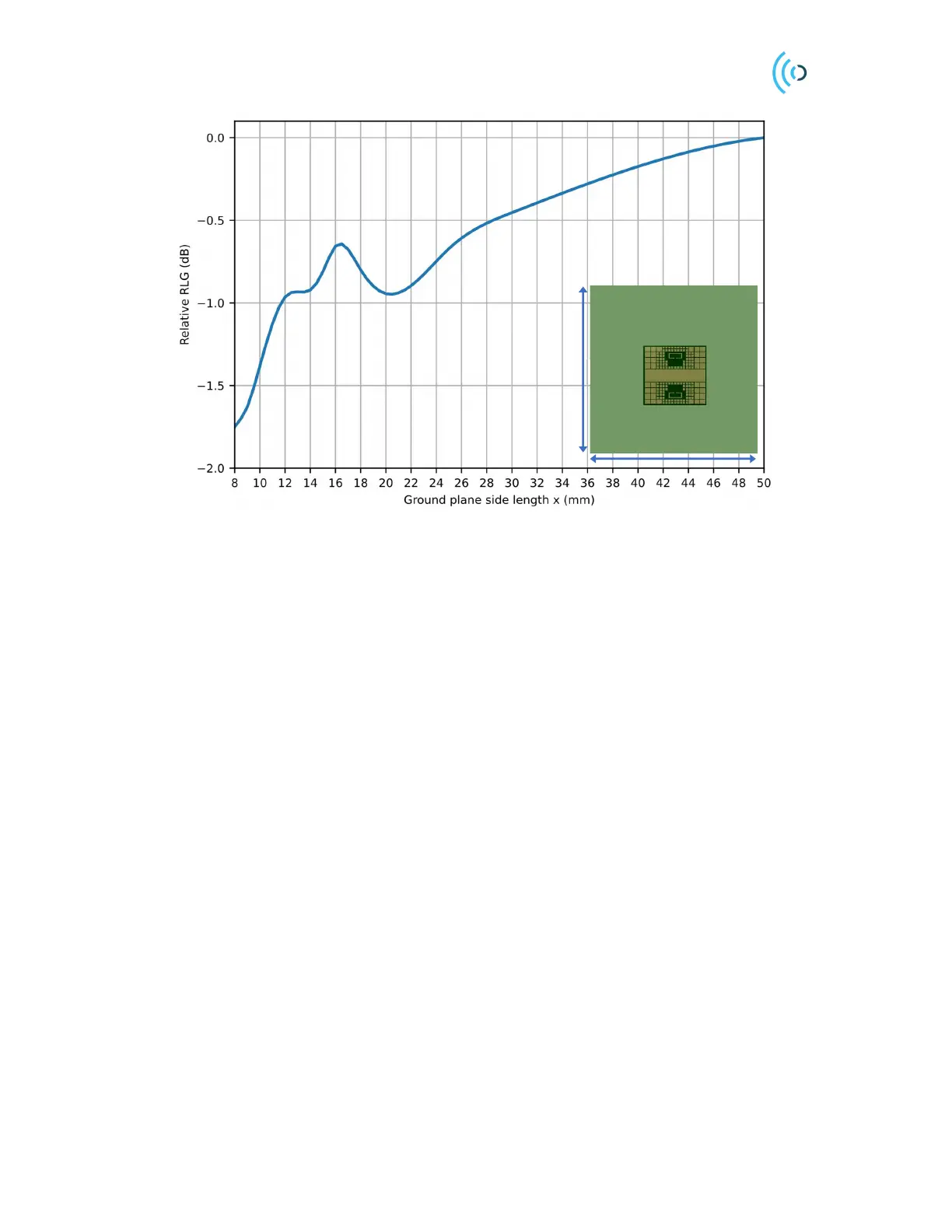
Figure 5. Simulated relative radar loop gain as a function of ground plane side length (x). Ground plane is a solid square
ground plane without routing.
In terms of regulatory compliance, any openings in the ground plane inside the A111/A121 BGA
footprint must be significantly smaller than the wavelength of the radiation that is being blocked, to
effectively approximate an unbroken conducting surface.
3.3.2 Impact of PCB routing and nearby components
As no RF components are required for the sensor integration, low-cost FR-4 type PCBs can generally
be used. However, for a symmetrical RLG pattern and maximum directivity, the following PCB design
rules should be considered:
- Whenever possible, place decoupling capacitors and the crystal on the opposite side of the PCB. In
other cases, the decoupling capacitors can be placed as in Figure 6b and the crystal placed some
distance away from the sensor. A small RLG loss of approximately 0.5 dB is seen when placing
decoupling capacitors (metric 1005 or smaller) as shown in Figure 7.
- Minimize amount of routing close to the sensor. This can be done by routing the signals to the sensor
with vias placed as close as possible to the sensor pads as shown in Figure 6. The ground plane area
x
 Loading...