1
3
AJA 3GDA 1x6 3G/HD/SD Reclocking Distribution Amplifier User Manual — Introduction
Introduction
The 3GDA is a miniature, low-cost 1x6 3G HD-SDI, HD-SDI, and SDI re-clocking
distribution amplifier. Featuring six separately buffered SDI outputs, the 3GDA
provides automatic input detection, re-clocking and cable equalization.
Features
•
SD/HD/3G-HD Distribution
•
Six Separately Buffered Outputs
•
Miniature Size
•
120m 3G cable equalization (1694 coax)
•
3G HD-SDI, HD-SDI or SDI input, auto-sensing
•
Passes all ancillary data
•
+5-18V power supply (power supply sold separately)
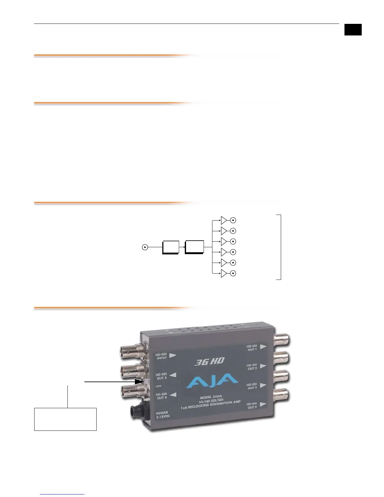
Block Diagram
3GDA Block Diagram
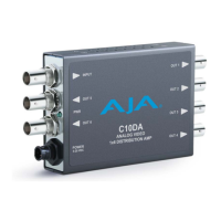
I/O Connections
3GDA, Side View
3G-HD-SDI, HD-SDI, or SD-SDI
with Embedded Audio
In
3G-HD-SDI, HD-SDI, or SD-SDI
with Embedded Audio Out
ReClock
Serial Video Out 1
Outputs pass
embedded audio
and metadata
Serial Video Out 2
Serial Video Out 3
Serial Video Out 4
Serial Video Out 5
Serial Video Out 6
Cable
EQ
3G/HD-SDI/SDI Input
3G/HD-SDI/SDI
+ 5 to 18VDC
Output 5
Power
Input
BNC
BNC
3G/HD-SDI/SDI
Output 6
BNC
LOCK LED
3G/HD-SDI/SDI
Output 1
BNC
3G/HD-SDI/SDI
Output 2
BNC
3G/HD-SDI/SDI
Output 3
BNC
3G/HD-SDI/SDI
Output 4
BNC
Green: Lock to SD
Red: Lock to HD or 3G