Do you have a question about the Akai AM-A402 and is the answer not in the manual?
Detailed safety precautions for service personnel, covering part replacement and wiring.
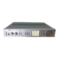
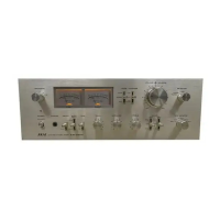
Technical specifications for AM-A102 and AM-A202 stereo integrated amplifiers.
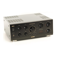
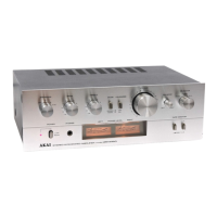
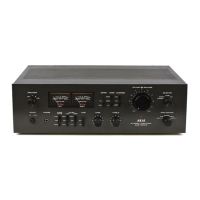
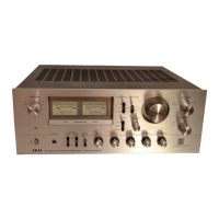
Technical specifications for AM-A302 and AM-A402 stereo integrated amplifiers.
Highlights safety critical components and the necessity of using recommended replacement parts.
High-level functional block diagram for AM-A102 and AM-A202 models.
High-level functional block diagram for AM-A302 and AM-A402 models.
Functional block diagram of the Pin Jack PCB for AM-A102/202.
Functional block diagram of the Equalizer PCB for AM-A302/402.
Functional block diagram of the Function PCB for AM-A302/402.
Functional block diagram of the Control PCB for AM-A302/402.
Functional block diagram of the Main PCB for AM-A302/402.
Detailed circuit schematic for the Pin Jack PCB.
Detailed circuit schematic for the Power Switch PCB.
Detailed circuit schematic for the Function PCB.
Detailed circuit schematic for the Filter PCB.
Detailed circuit schematic for the Control PCB.
| Speaker Load Impedance | 4 - 16 ohms |
|---|---|
| Power Output | 40 Watts per channel (8 ohms) |
| Input Sensitivity | 150mV (line) |
| Signal to Noise Ratio | 90 dB |
| Output | Speaker outputs |
| Input Impedance | 47 kOhm |