Sync In Wordclock Modification for RL Main PCB Rev. C
(August 29, 2001)
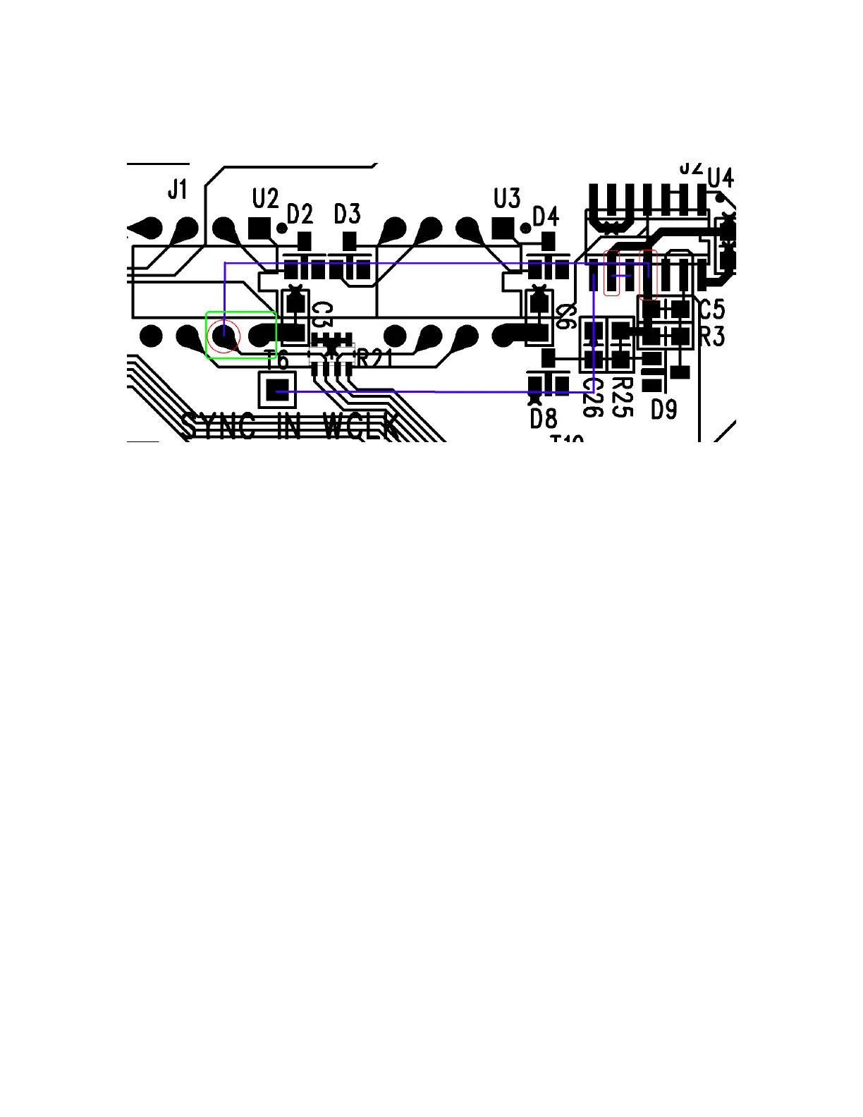
Fig. 1: Circuit Modification Diagram
Steps:
1. Cut U2 pin 7 (red circle) as close to PCB as possible.
Bend pin approximately straight out.
2. Lift U4 pins 9 & 11 (red rectangles) from the PCB.
Be careful to lift pins straight to keep from breaking
them off.
3. Connect 220 Ohm resistor between pins 7 and 8 of U2
(green rectangle).
4. Short pins 9 and 10 of U4 with solder blob or wire
wrap wire (blue line).
5. Connect U2 pin 7 to U4 pin 11 with wire wrap wire
(blue line).
6. Connect U4 pin 8 to T6 (SYNC IN WCLK) with wire
wrap wire (blue line).
7. Secure wires to PCB with hot melt glue or silicone
adhesive.