The ALINX AXU15EGB is an FPGA development board featuring a ZYNQ UltraScale+ MPSoC EG family chip (XCZU15EG-2FFVB1156I). This board is designed for high-speed data processing, deep learning, artificial intelligence, and industrial control applications, making it suitable for professional ZYNQ development.
Function Description:
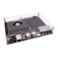
The AXU15EGB development board integrates a core board and a carrier board. The core board, ACU15EG, houses the ZYNQ UltraScale+ MPSoC EG chip, which combines a processing system (PS) and programmable logic (PL). The PS side includes a dual-core ARM Cortex-A53 and two Cortex-R5 processors, while the PL side offers extensive programmable logic for custom designs.
The board provides a rich set of interfaces for various applications:
- M.2 Interface: A PCIe x1 standard M.2 interface (M key slot, PCIe type SSD only) for connecting M.2 SSD solid-state drives, supporting communication speeds up to 6Gbps.
- DisplayPort (DP) Interface: A standard DisplayPort V1.2a output for video display, supporting up to 4K x 2K@30Fps output and various video formats (Y-only, YCbCr444, YCbCr422, YCbCr420, RGB) with 6, 8, 10, or 12 bits per color.
- USB 3.0 Interfaces: Four USB 3.0 ports supporting HOST mode with data transmission speeds up to 5.0Gbps. It uses an external USB3320C chip for high-speed USB3.0 and USB2.0 data communication.
- Gigabit Ethernet Interfaces: Two 10/100/1000M Ethernet RJ-45 interfaces using JL2121-N040IRNX PHY chips, one connected to the PS and the other to the PL.
- USB UART Interfaces: Two USB-UART ports for serial data communication, one connected to the PS and one to the PL, using Silicon Labs CP2102GM chips.
- Micro SD Card Slot: For storing BOOT programs, Linux operating system kernels, file systems, and user data.
- MIPI Camera Interface: A 15-pin FPC connector for MIPI OV5640 camera modules (AN5641), supporting 2 LANE data and 1 pair of clock.
- FMC Interface: A standard FMC HPC expansion port for connecting various FMC modules (HDMI input/output, binocular camera, high-speed AD modules), providing 36 pairs of differential IO signals and 8 pairs of GTX transceivers.
- CAN Communication Interfaces: Two CAN bus interfaces using TI's SN65HVD232 chip.
- 485 Communication Interfaces: Two 485 communication interfaces using MAXIM's MAX3485 chip.
- JTAG Debugging Interface: A 10-pin 0.1 spacing standard JTAG port for FPGA program download and debugging, with protection diodes to prevent damage.
- 40-Pin Expansion Header: A 0.1-inch pitch expansion port (J50) for connecting external ALINX modules or custom circuits, providing 34 IOs, 1 channel 5V, 2 channels 3.3V power, and 3 grounds.
Important Technical Specifications:
Core Board (ACU15EG):
- FPGA Chip: Xilinx Zynq UltraScale+ MPSoC EG family, XCZU15EG-2FFVB1156I (industrial grade, speed grade -2, package FFVB1156).
- DDR4 SDRAM:
- PS side: 4 Micron MT40A512M16GE chips, 64-bit data bus, 4GB capacity, up to 1200MHz (2400Mbps data rate).
- PL side: 2 Micron MT40A512M16GE chips, 32-bit data bus, 2GB capacity, up to 1200MHz (2400Mbps data rate).
- Flash Memory:
- 8GB eMMC FLASH (MTFC8GAKAJCN-4M).
- Two 256Mbit QSPI FLASH (MT25QU256ABA1EW9, Winbond).
- Clock Sources:
- PS system: 33.333MHz active crystal oscillator.
- PL logic: 200MHz differential crystal oscillator for DDR4 controller.
- RTC: 32.768KHz passive crystal.
- Power Supply: DC12V input. Core power (0.85V) provided by 2 MYMGM1R824 chips (50A current). Other power supplies generated by TPS6508640 PMIC.
- I/O Expansion: Four 120-pin Panasonic AXK5A2137YG board-to-board connectors (J29/J30/J31/J32) expanding PS MIO ports, 4 pairs of PS MGT high-speed transceivers, 16 GTH transceivers, and almost all PL I/O ports (HP I/O: 96, HD I/O: 84).
- Dimensions: 3.15 x 2.36 inches.
Carrier Board:
- USB 3.0 Hub Chip: GL3523T.
- USB PHY Chip: USB3320C.
- Ethernet PHY Chip: JL2121-N040IRNX.
- USB-UART Chip: Silicon Labs CP2102GM.
- SD Card Level Shifter: TXS02612.
- CAN Transceiver Chip: TI SN65HVD232C.
- 485 Transceiver Chip: MAXIM MAX3485.
- EEPROM: 24LC04 (4Kbit, I2C interface).
- Temperature Sensor: LM75 (0.5-degree accuracy, I2C interface).
- RTC: Built-in real-time clock with a battery socket for LR1130 coin battery.
- LEDs: 5 LEDs (1 on core board, 4 on carrier board), including power indicators, DONE configuration indicator, and user indicators.
- Keys: 3 keys (1 Reset KEY, 2 User KEYs).
- DIP Switch: 4-digit DIP switch (SW1) for configuring startup modes (JTAG, QSPI FLASH, EMMC, SD2.0).
- Power Distribution: Converts 12V to +5V, +3.3V, +1.8V, and +1.2V using TPS54620 and MP1482 chips.
- Fan: ALINX customized fan for cooling the ZU15EG chip, controlled by the ZYNQ chip.
- Dimensions: 180.0 mm x 135.0 mm.
Usage Features:
- Flexible Boot Options: Supports multiple startup modes (JTAG, QSPI FLASH, EMMC, SD2.0 card) configurable via a 4-digit DIP switch, allowing users to select the appropriate boot method for their application.
- Extensive Connectivity: The wide array of interfaces (M.2, DisplayPort, USB 3.0, Gigabit Ethernet, MIPI, FMC, CAN, 485, USB UART) enables the board to connect to a diverse range of peripherals and systems, facilitating complex designs.
- Secondary Development Support: The core board's compact size and comprehensive I/O expansion make it highly suitable for integration into custom designs and secondary development projects.
- High-Speed Data Handling: The DDR4 SDRAM on both PS and PL sides, along with high-speed transceivers (MGT, GTH), ensures efficient handling of large data volumes and high-bandwidth applications.
- Real-time Clock Functionality: The integrated RTC provides accurate timekeeping, supported by a coin battery for continuous operation even when the system is powered off.
Maintenance Features:
- Temperature Monitoring: An on-board LM75 temperature and humidity sensor allows monitoring of the environment around the FPGA development board, aiding in thermal management.
- Cooling System: An ALINX customized fan and heat sink are pre-installed to prevent the ZU15EG chip from overheating, ensuring stable operation. The fan's operation is controlled by the ZYNQ chip.
- JTAG Debug Port: A dedicated JTAG port with protection diodes simplifies program download and debugging, minimizing the risk of damage to the ZYNQ chip during development.
- EEPROM for Configuration: An EEPROM (24LC04) is available for storing configuration data, which can be accessed via the I2C bus.
- Clear Pin Assignments: Detailed pin assignment tables for all interfaces and connectors are provided in the manual, simplifying hardware debugging and custom circuit design.