S19 Maintenance Guide
13
Figure 5-16
d-2) The second case; the test time is almost twice as long as the good board (sometimes the value of X will change every time you test,
and sometimes X=0); at this time, the log usually has the following information (the red number is not 13, depending on which seat the
hashboard tester is connected to); during the test, assume that the domain voltage of all the fields in front of the abnormal position is
almost less than 0.3V, and the domain voltage of the back fields are almost all higher than 0.38V. This situation is caused by the chip not
being soldered well, usually 1.8V, 0.8V, RXT, CLK are not soldered well. It is recommended to directly measure the domain voltage to
locate which domain is the problem. The 1V8 and RO short-circuit method used in section a) can also locate the abnormal position;
Figure 5-17
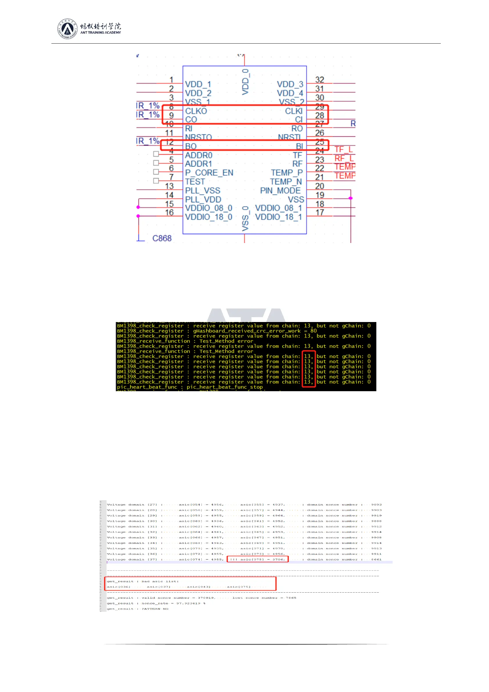
5. Phenomenon: Single board Pattern NG, indicating that the response nonce data is incomplete (PT2 station)
PatternNG is caused by the large difference between the characteristics of the chip and other chips. At present, it is found that the chip die
is damaged, so just replace the chip. According to the log information, the replacement rules are as follows:
If the appearance of the chip is not damaged, just replace the chip with the lowest response rate in each domain. The following figure
shows one of the test logs, it can be seen from the log that the response rate of four chips asic[36][37][43][75] is low. 36 and 37 are in the
same domain, so replace the one with the lower nonce in 36 and 37. At the same time, replace the 43 and 75.
PS: Special attention shall be paid to that the numbers of domain and asic start from 0
Figure 5-18
 Loading...