APW9 Power Supply Maintenance Guide
8
VCC-PWM main control chip driver circuit:
LLC--- main transformer buck DC conversion circuit:
Synchronous rectifying filter main output 14.5v-21v circuit port:
Sample feedback voltage stabilization:
PWM main switch MOS circuit:
Parallel output 12V circuit port:
PIC recording and communication control circuit:
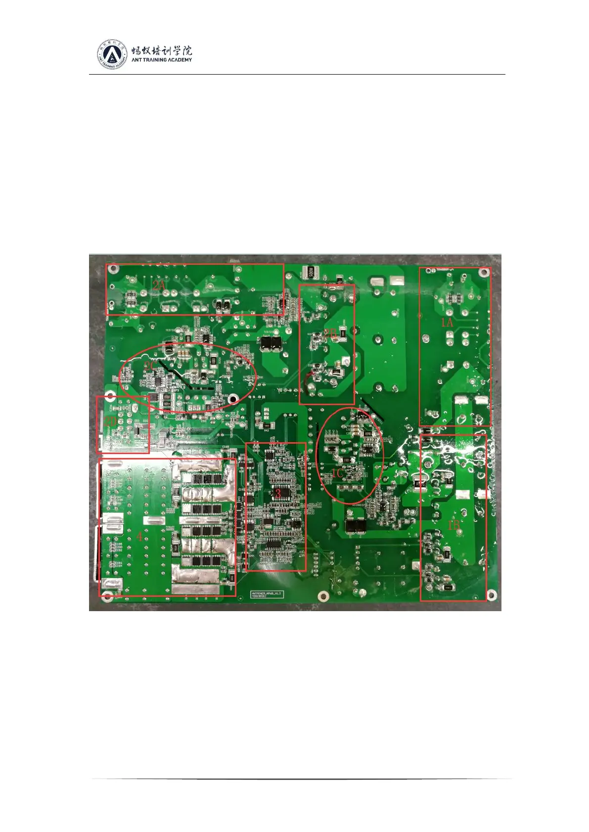
2.2 Power PCBA board layout
Layout description: 1A-- first AC input and EMI circuit, 1B- PFC and main shunt MOS
circuit, 1C-- 12V auxiliary and VCC circuit.
 Loading...