Do you have a question about the Casio TV-600B and is the answer not in the manual?
Explains the DC tuning voltage generation circuit and its output.
Lists items and test point locations for adjustments on the Linear PCB.
Details the clock adjustment procedure and test points for the A/D PCB.
Circuit diagram for the linear section of the TV.
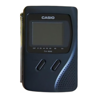
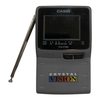
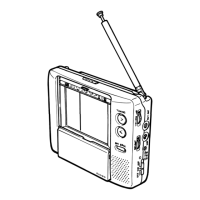
This document is a service manual and parts list for the Casio TV-600B Pocket Television, published in December 1994. It provides detailed information for maintenance, adjustment, and repair of the device.
The Casio TV-600B is a pocket television designed for receiving VHF-L, VHF-H, and UHF signals. It incorporates a DC-DC converter for power supply, generating various voltages required for its operation, including main voltage, tuning voltage, and display voltage. The device features a tuning voltage generator (IC500 MSC1169MS-K) that selects the appropriate VHF-L, VHF-H, or UHF band based on input pulses from IC700, and outputs the corresponding tuning voltage (BT).
Power Supply Voltages (Table 2):
Integrated Circuits (IC/LSI Lead Identification):
Transistors:
Waveforms (Examples):
The TV-600B is designed for portable use, indicated by its "Pocket Television" designation. Its tuning system allows for reception across different television frequency bands. The detailed circuit diagrams and adjustment procedures suggest that the device is intended for a broad range of users, from casual viewers to those requiring specific channel tuning. The inclusion of an external antenna jack (JK200 EXT ANT) implies flexibility in signal reception, allowing for improved performance with an external antenna.
The manual provides comprehensive instructions for adjustment and troubleshooting, making it a valuable resource for technicians.
Adjustment Procedures:
Test Point Locations:
Exploded View / Disassembly: The manual includes an exploded view diagram (Figure 4) with numbered components (1-20 and sub-components like 8-1, 8-2, etc.) to facilitate disassembly and reassembly. This is crucial for accessing internal components for repair or replacement.
Printed Circuit Boards (PCBs): Detailed top and bottom views of the Linear PCB and A/D PCB are provided, showing the layout of components, test points, and adjustment points. This visual guide is essential for identifying specific parts and performing accurate adjustments.
Wiring Diagram: A wiring diagram illustrates the connections between the A/D PCB and the Linear PCB, indicating the numbered pins (1-17) for proper interconnection during assembly or repair.
Parts List: The manual includes an electrical parts list and a mechanical parts list (though not shown in the provided excerpt), which would be vital for ordering replacement components.
Overall, the Casio TV-600B service manual is a comprehensive guide for maintaining and repairing the device, offering detailed technical specifications, adjustment procedures, and visual aids for component identification and assembly.
| Brand | Casio |
|---|---|
| Model | TV-600B |
| Category | Portable TV |
| Language | English |