25
3.
2.3.6 1st
Null Detector
The 1st null detector comprises a
low noise amplifier,
M22, an inverting configuration, where
the
dc
gain is con-
trolled
by the ratio of R59 to R28
for small inputs.
For
larger
inputs from the integrator the clamp
diodes,
D1
and
D3,
prevent the amplifier from saturating.
During
REF 1 the non-inverting
input is offset by
approximately
lOmV to determine
the point at which
REF
2
is applied (after counting is synchronised). In REF
2
the
offset reduces
by a
factor of
16
giving the null
reference
point.
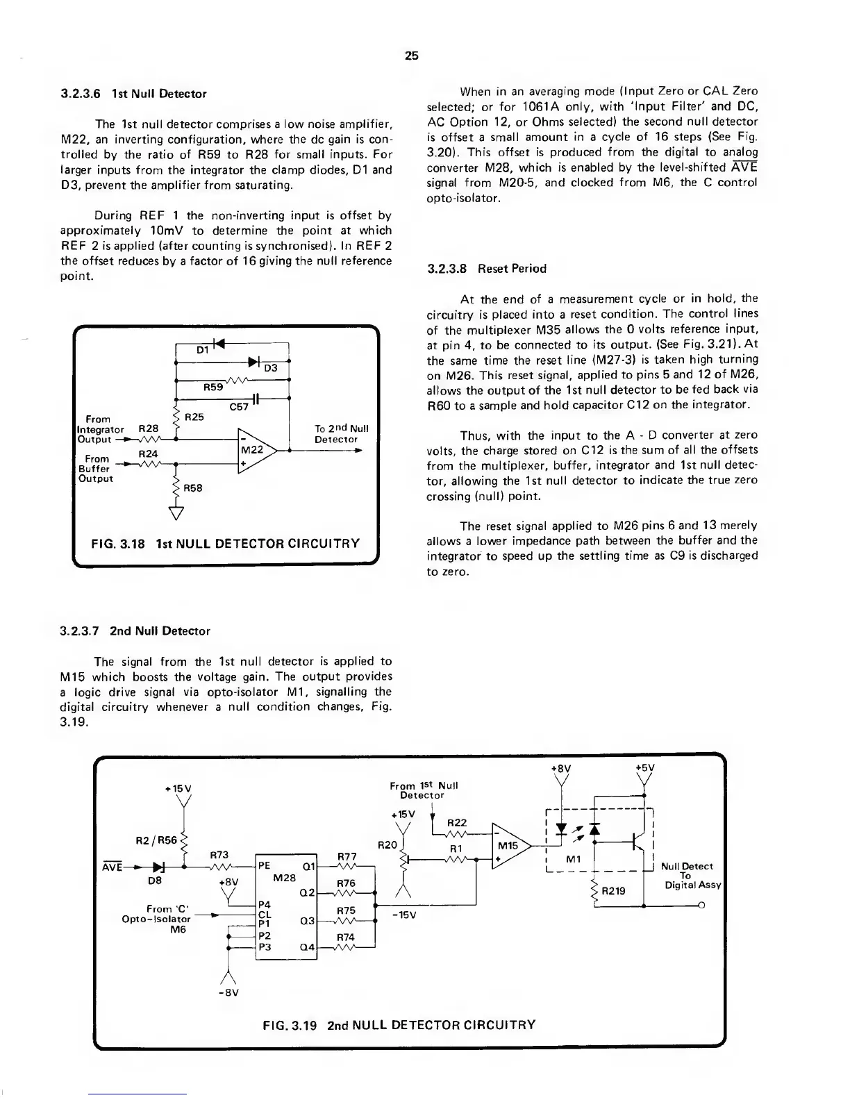
3. 2.3.7 2nd Null Detector
The signal from the 1st null
detector is
applied to
Ml
5
which
boosts
the voltage
gain. The output
provides
a
logic drive
signal via opto-isolator
Ml,
signalling the
digital
circuitry whenever
a
null
condition changes.
Fig.
3.19.
When
in an
averaging mode
(Input
Zero or
CAL
Zero
selected; or for 1061A
only,
with 'Input
Filter'
and DC,
AC
Option
12,
or Ohms
selected) the
second null detector
is offset
a
small amount
in
a
cycle of 16 steps
(See Fig.
3.20).
This offset is produced
from
the
digital to analog
converter
M28,
which is enabled by the
level-shifted AVE
signal
from M20-5, and
clocked from M6, the
C
control
opto-isolator.
3.2.3.S Reset
Period
At the
end of a
measurement
cycle or in hold,
the
circuitry is
placed
into
a
reset
condition.
The
control
lines
of
the
multiplexer M35
allows the 0
volts
reference
input,
at pin
4,
to
be
connected to
its output.
(See
Fig,
3.21).
At
the same
time the reset
line (M27-3)
is
taken
high
turning
on M26.
This reset
signal,
applied to pins 5
and 12
of M26,
allows the
output of the 1st
null
detector to
be fed
back
via
R60
to a
sample and
hold
capacitor Cl 2
on the
integrator.
Thus, with the
input to
the
A
-
D
converter at
zero
volts, the
charge stored
on
C12
is
the sum of
all the
offsets
from the
multiplexer,
buffer,
integrator and 1st
null detec-
tor, allowing
the 1st
null detector to
indicate
the true
zero
crossing
(null)
point.
The reset
signal applied to
M26 pins 6
and 13
merely
allows a
lower impedance
path
between the
buffer and
the
integrator to
speed
up
the
settling time
as C9
is discharged
to
zero.
 Loading...