27
PREAMPLIFIER, SCALING AND
FREQUENCY
COMPENSATION
RMS CONVERTER
To A-D
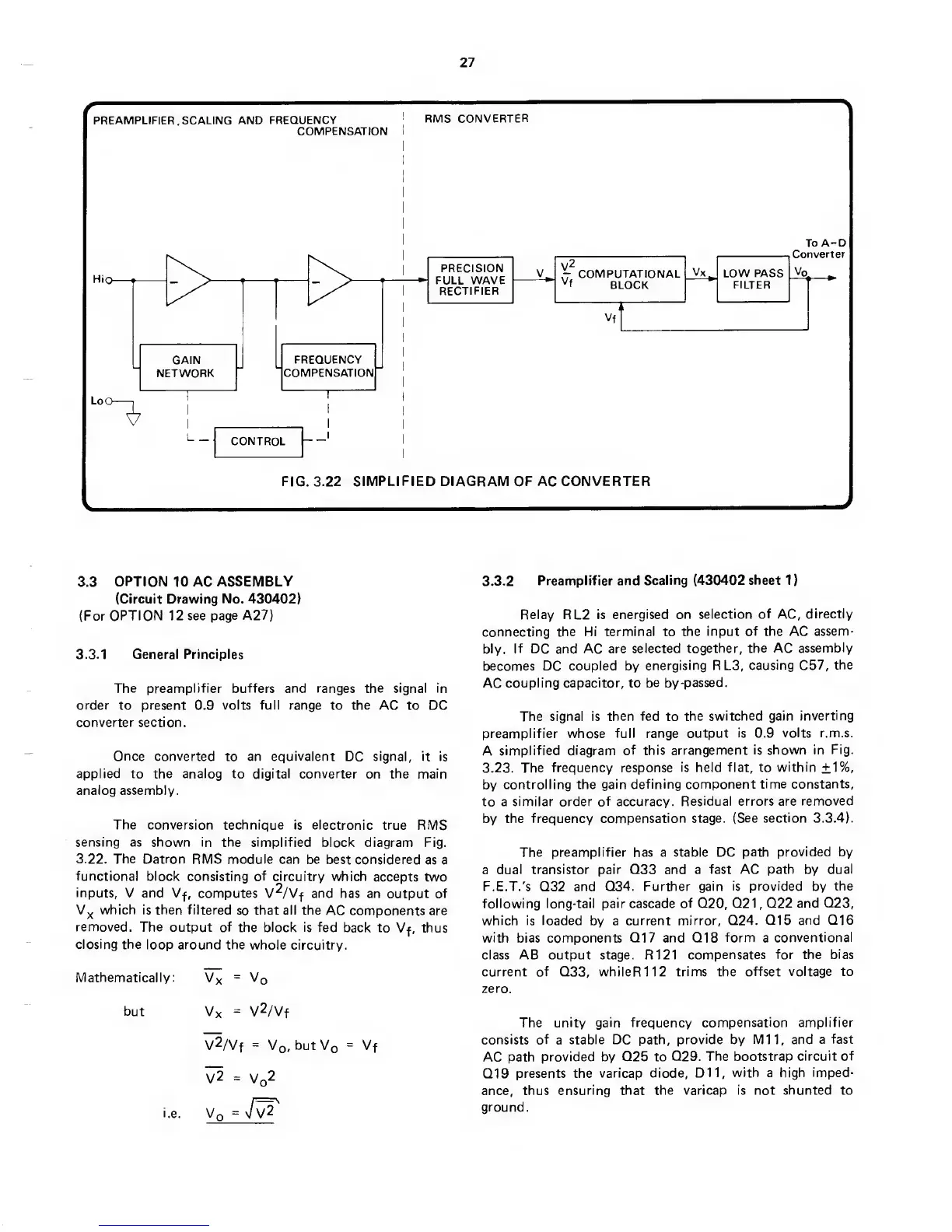
FIG. 3.22
SIMPLIFIED
DIAGRAM OF AC CONVERTER
3.3
OPTION
10
AC ASSEMBLY
(Circuit Drawing
No.
430402)
(For
OPTION 12 see
page
A27)
3.3.1 General Principles
The preamplifier buffers and ranges the signal in
order
to
present
0.9
volts full range
to
the
AC to DC
converter section.
Once converted
to an
equivalent
DC signal, it is
applied to the analog to digital converter on the main
analog
assembly.
The conversion technique is electronic true
RMS
sensing as shown in the simplified
block diagram Fig.
3.22. The
Datron
RMS module can be
best considered
as a
functional
block consisting of circuitry
which accepts
two
inputs,
V and
Vf,
computes
V^/Vf
and has an output of
which is then filtered
so that all the
AC components are
removed. The
output of the block is
fed back to
Vf,
thus
closing the
loop around the
whole circuitry.
Mathematically:
Vx
=
Vq
but
Vx
=
V2/Vf
V2/Vf
=
Vo,
but
Vo
=
Vf
V2
=
Vo2
3.3.2
Preamplifier and
Scaling (430402
sheet
1
)
Relay
RL2
is
energised on selection
of
AC,
directly
connecting
the Hi
terminal
to
the input
of
the AC
assem-
bly. If DC and AC are
selected together,
the
AC
assembly
becomes DC coupled by
energising RL3,
causing
C57,
the
AC
coupling capacitor, to
be
by
-passed.
The signal
is then fed
to
the
switched gain
inverting
preamplifier whose
full range output
is
0.9
volts r.m.s.
A
simplified
diagram of this arrangement
is shown in
Fig.
3.23. The
frequency response
is held flat, to
within
±1%,
by
controlling the
gain defining component
time constants,
to a similar order of accuracy.
Residual
errors are removed
by the frequency
compensation stage. (See
section
3.3.4).
The
preamplifier
has a
stable
DC
path provided by
a
dual transistor pair
Q33
and a
fast
AC path by
dual
F.E.T.'s
Q32
and Q34. Further gain
is provided
by
the
following long-tail pair cascade
of
Q20,
Q21,
Q22 and
Q23,
which is loaded
by a
current mirror, Q24. Q15
and Q16
with bias
components
Q17 and
Q18
form
a
conventional
class AB output stage. R121
compensates for the
bias
current of
Q33,
whileR112 trims the
offset voltage to
zero.
The unity gain frequency compensation
amplifier
consists of
a
stable DC path,
provide
by Mil, and
a fast
AC
path provided by Q25 to
Q29.
The bootstrap circuit of
Q19
presents the
varicap diode.
Dll, with a high
imped-
ance, thus
ensuring that the varicap is not shunted to
ground.
 Loading...