28
/
\
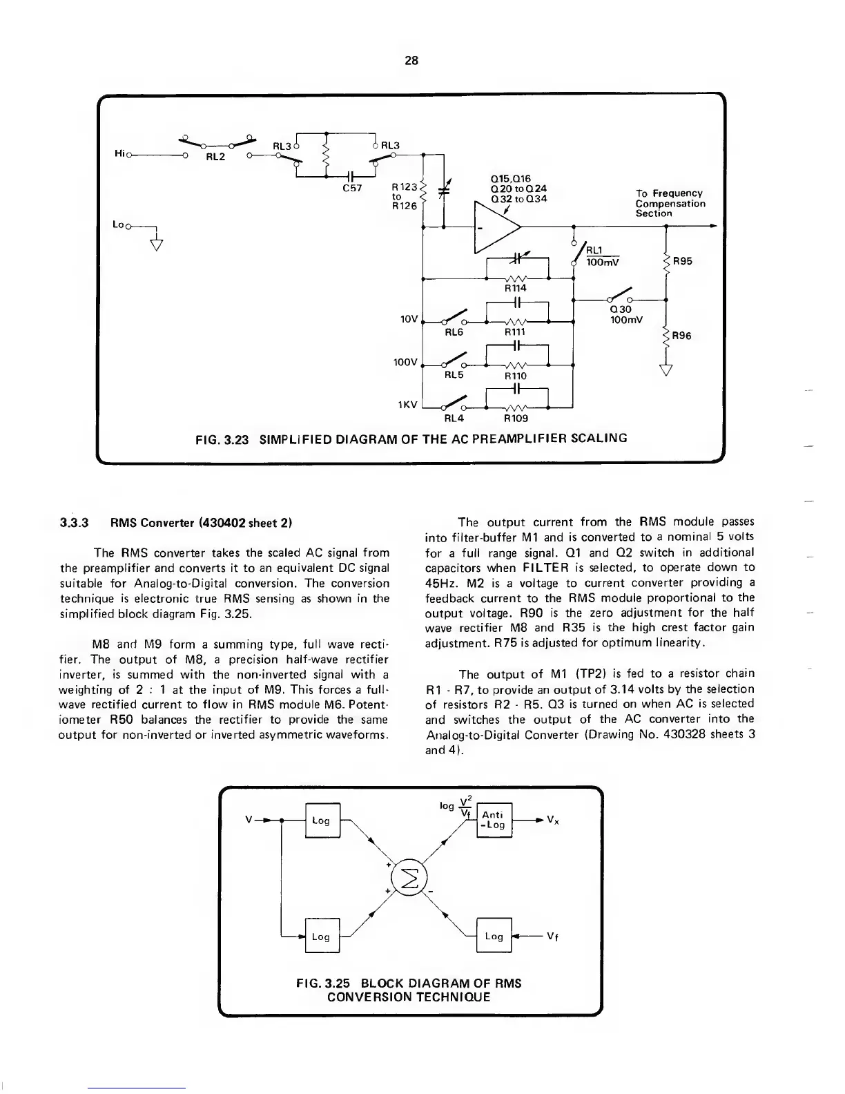
FIG. 3.23
SIMPLIFIED DIAGRAM OF THE AC
PREAMPLIFIER
SCALING
J
3.3.3 RMS
Converter
(430402
sheet
2)
The RMS converter
takes the scaled AC signal
from
the preamplifier and converts it to an
equivalent
DC
signal
suitable for Analog-to-Digital
conversion. The conversion
technique
is
electronic true RMS sensing as shown
in the
simplified block diagram Fig.
3.25.
M8
and
M9
form
a
summing type, full wave recti-
fier. The output of
M8,
a precision
half-wave rectifier
inverter, is
summed
with
the
non-inverted signal with
a
weighting of
2
;
1 at the input
of
M9. This
forces
a full-
wave rectified current to flow in
RMS
module
M6.
Potent-
iometer
R50 balances
the rectifier to provide the same
output
for non-inverted or inverted
asymmetric
waveforms.
The output
current
from the RMS
module passes
into
filter-buffer Ml and
is
converted to
a
nominal
5
volts
for a
full range signal. Q1
and Q2 switch
in additional
capacitors when
FILTER is selected,
to
operate down to
45Hz. M2
is a
voltage to
current
converter
providing a
feedback
current
to
the RMS
module
proportional to
the
output
voltage. R90
is the
zero
adjustment
for
the
half
wave
rectifier
M8
and R35
is the high crest
factor gain
adjustment.
R75
is adjusted
for optimum
linearity.
The
output
of M1
(TP2)
is fed to a
resistor
chain
R1
-
R7,
to provide
an output
of 3.14
volts by
the selection
of
resistors
R2
-
R5.
Q3
is
turned on when AC
is selected
and switches
the output
of the AC
converter
into the
Analog-to-Digital
Converter
(Drawing No,
430328
sheets 3
and
4).
 Loading...