39
3.8.3
Analog
to
Digital
Conversion
(Digital Section)
3.8.3.1
General Principle
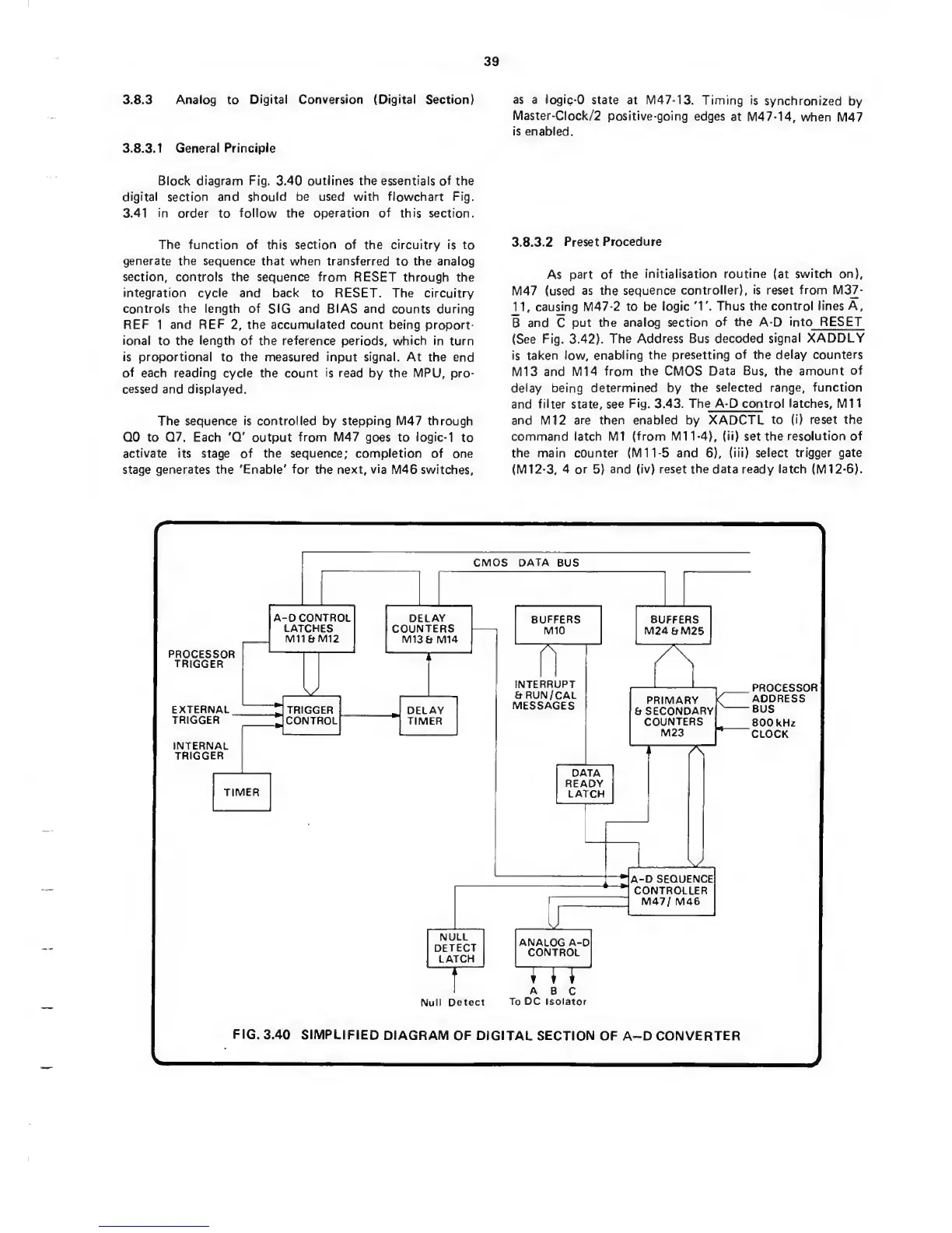
Block diagram Fig. 3.40 outlines the essentials of the
digital section and should be used with flowchart Fig.
3.41
in
order
to
follow the
operation of
this section.
The function of
this
section of
the circuitry is to
generate the sequence
that
when transferred
to the analog
section, controls the sequence from RESET
through the
integration cycle and
back to RESET. The circuitry
controls the length of
SIG
and BIAS
and counts during
REF 1
and REF
2,
the
accumulated
count being proport-
ional
to
the length of
the
reference
periods, which in turn
is proportional
to
the measured
input
signal.
At the end
of each reading cycle the count is read
by
the MPU,
pro-
cessed
and
displayed.
The sequence is
controlled
by
stepping
M47
through
QO to Q7. Each
'Q'
output
from M47
goes to
logic-1
to
activate
its stage
of
the sequence;
completion of
one
stage
generates the 'Enable' for the next, via M46
switches.
as a logic-0
state at M47-13.
Timing is
synchronized
by
Master-Clock/2
positive-going
edges
at M47-14,
when
M47
is enabled.
3.8.
3.
2
Preset Procedure
As
part of the
initialisation
routine
(at
switch on),
M47 (used
as the sequence
controller), is reset from M37-
11,
cau^ng M47-2
to be
logic
'1'.
Thus the control lines A,
B
and
C
put the
analog section
of the A-D
int
o RESET
(See
Fig.
3.42).
The
Address Bus decoded
signal XADDLY
is taken low, enabling
the
presetting of the delay counters
M13 and M14
from the CMOS Data
Bus, the amount
of
delay being
determined
by
the
selected range, function
and
filter
state, see
Fig. 3.43. The A-D control
latches. Mil
and
Ml 2
are then enabled
by
XADCTL
to (i)
reset
the
command
latch Ml (from Ml 1-4),
(ii)
set
the resolution of
the
main
counter
(Ml
1-5
and
6),
(iii) select
trigger
gate
(M12-3, 4 or
5)
and (iv) reset the data ready latch (M12-6).
r
CMOS DATA
BUS
PROCESSOR
ADDRESS
BUS
800kHz
CLOCK
Null
Detect
To DC Isolator
V.
J
FIG.
3.40 SIMPLIFIED
DIAGRAM
OF DIGITAL
SECTION OF
A-D
CONVERTER
 Loading...