Please read this instruction carefully before use.
DO NOT tough any terminal when the power is switched on. Switch off the power before wiring.
DVP06AD-S is an OPEN-TYPE device and therefore should be installed in an enclosure free of airborne dust,
humidity, electric shock and vibration. The enclosure should prevent non-maintenance staff from operating the device
(e.g. key or specific tools are required to open the enclosure) in case danger and damage on the device may occur.
DO NOT connect input AC power supply to any of the I/O terminals; otherwise serious damage may occur. Check all
the wiring again before switching on the power.
DO NOT touch any internal circuit in 1 minute after the power is switched off.
Make sure the groud terminal is correctly grounded in order to prevent electromagnetic interference.
Introduction
Model Explanation & Peripherals
Thank you for choosing Delta DVP series. The analog signal input module DVP06AD-S is able to receive 6
points of external analog signal inputs (both in voltage and current) and convert the signals into 14-bit
digital ones. It is able to read and write the data in the module through FROM/TO instructions given by the
program of DVP-PLC SS/SA/SX/SC/SV series MPU. There are 49 16-bit control registers in the module.
The user can select voltage or current output by wiring. Range of voltage output:
±
10V DC (resolution:
1.25mV). Range of current output:
±
20mA (resolution: 5µA).
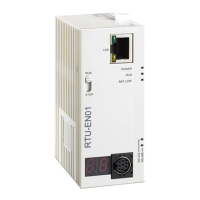
Product Profile & Outline
1.
POWER, ERROR, A/D indicator
2.
Extension unit/module mounting h ole
5.
Extension unit/module connection port
Extension unit/module fixing clip
8.
RS-485 communication port
10.
Extension unit/module fixing notch
11.
Power input port
3.0090.00
3.00
25.20
60.00 3.40
1
2
12
3
4
6
8
2
5
7
10
9
11
60.00
3.00
Extension unit/module connection port
External Wiring
104 .7K
250
-20mA ~+20mA
V+
I+
COM
Shield ing cab le*1
Curre nt input
Sys tem ground ing
Eart h
Conn ected to
ter minal
of the p ower modul e
Cover ter
DVP06AD-S
*1: When performing analog input, p
lease isolate other power wirings.
*2: When connecting to current signals, please make sure to short-circuit “V+” and “I+” terminals.
*3: Please connect the terminal on both the power module and DVP06AD-S to the system earth point and ground the
system contact or connect it to the cover of power distribution cabinet.
*4: If the ripples at the loaded input terminal are too significant that causes noise interference on the wiring, connect the
wiring to 0.1 ~ 0.47µF 25V capacitor.
Note: DO NOT wire empty terminals
Specifications
Functions
Analog/Digital
(6A/D) module
Voltage input Current input
Power supply voltage 24V DC (20.4V DC ~ 28.8V DC) (-15% ~ +20%)
Analog input channel 6 channels/module
Range of analog input ±10V ±20mA
Range of digital
conversion
±8,000 ±4,000
Resolution 14 bits (1
LSB
=1.25mV) 13 bits (1
LSB
=5µA)
Input impedance 200KΩ or more 250Ω
Overall accuracy
±0.5% when in full scale (25°C, 77°F)
±1% when in full scale in the range of 0 ~ 55°C, 32 ~ 131°F
Response time 3ms × the number of channels
Isolation Isolation between digital area and analog area. No isolation among channels.
Range of absolute input ±15V ±32mA
Digital data format 13 significant bits out of 16 bits are available; in 2’s complement.
Average function Yes. Available for setting up in CR#2 ~ CR#7; range: K1 ~ K20.
Self-diagnosis Upper and lower bound detection/channel
Communication mode
(RS-485)
ASCII/RTU mode.
Communication speed: 4,800/9,600/19,200/38,400/57,600/115,200
ASCII data format: 7-bit, even bit, 1 stop bit (7, E, 1)
RTU data format: 8-bit, even bit, 1 stop bit (8, E, 1)
RS-485 cannot be used when connected to PLC MPU in series.
When connected to
DVP-PLC MPU in series
The modules are numbered from 0 to 7 automatically by their distance from MPU.
Maximum 8 modules are allowed to connect to MPU and will not occupy any digital I/O
points.
Others
Power supply
Max. rated power
consumption
24V DC (20.4V DC ~ 28.8V DC) (-15% ~ +20%), 2W, supplied by external power.
Environment
Operation/storage
Operation: 0°C ~ 55°C (temperature); 50 ~ 95% (humidity); pollution degree 2.
Storage: -25°C ~70°C (temperature); 5 ~ 95% (humidity).
Vibration/shock
immunity
International standards: IEC 61131-2, IEC 68-2-6 (TEST Fc)/IEC 61131-2 & IEC
68-2-27 (TEST Ea)
Mounting Arrangements and Wiring Notes
Control Registers
CR
#
#0 H’4000
○
R Model name
Set by the system. Data length: 8 bits (b7 ~ b0).
DVP06AD-S m odel code =H’C8.
Reserved CH6 CH5 CH4 CH3 CH2 CH1
#1 H’4001
○
R/W Input mode setting
Input mode: Default=H’0000.
Mode 0: Voltage input (-10V ~ +10V)
Mode 1: Voltage input (-5V ~ +10V)
Mode 2: Current in put (-12mA ~ +20mA)
Mode 3: Current in put (-20mA ~ +20mA)
CR#1: The working mode of the 6 channels in the analog input module. There are 4 modes for each channel which can
be set up separately. For example, if the user needs to set up CH1: mode 0 (b2 ~ b0=00) and CH2: mode 1 (b5 ~ b3=01),
CH3: mode 2 (b8 ~ b6=10), CH4: mode 3 (b11 ~ b9=11), CH5: mode 0 (b11 ~ b9=00), CH6: mode 1 (b11 ~ b9=01), CR#1
has to be set as H’04EA and the higher bits (b12 ~ b15) have to be reserved. Default value=H’0000.
#2
CH1 ~ CH6
Average times setting
CH6 CH5
CR#2 ~ CR#4: Range of settings in CH1 ~ CH 6: K1 ~ K20. The settings of average tim es of the signals at CH1 ~ CH6.
Range: K1 ~ K20. For example, if the average time at CH1 is to be set as K10 and CH2 as K18, CR#2 has to be set as
H’120A. CR#3 ~ 4 apply the same rule. The default se tting of each channel=K10. Default settings of CR#2 ~ CR#4 are all
R CH6 input average
Average of input signals at CH1 ~ CH6
CR#6 ~ CR#11: The average of the signals at CH1~C H6 obtained from the settings in C R#2~CR#4. For example, if the
settings in CR#2~CR#4 is 10, the content in CR#6~CR#11 will be the average of the most recent 10 signals at CH1 ~CH6.
How to install DIN rail
DVP-PLC can be secured to a cabinet by using the DIN rail of
35mm in height and 7.5mm in depth. When mounting PLC to
DIN rail, be sure to use the end bracket to stop any side-to-side
movement of PLC and reduce the chance of wires being loosen.
A small retaining clip is at the bottom of PLC. To secure PLC to
DIN rail, place the clip onto the rail and gently push it up. To
remove it, pull the retaining clip down and gently remove PLC
from DIN rail, as shown in the figure.
Please install PLC in an
enclosure with sufficient
space around it to allow
heat dissipation as shown
in the figure.
DVP
MP
D
D
DD
D > 50 mm
1. Use 22-16AWG (1.5mm) single or multiple core wire on I/O wiring terminals. The
specification of the terminal is shown in the figure on the left. The PLC terminal
screws shall be tightened to 1.95 kg-cm (1.7 in-lbs).
2. DO NOT place the I/O signal wires and power supply wire in the same wiring duct.
3. Use 60/75 ºC copper wires only.
CR
#
R CH1 input present value
#13
R CH2 input present value
#14
R CH3 input present value
#15
R CH4 input present value
#16
R CH5 input present value
#17
R CH6 input present value
Present value of in put signals at CH1 ~ CH6
#18
Adjusted OFFSET value of CH 1
H’4014
○
R/W Adjusted OFFSET value of CH 3
Adjusted OFFSET value of CH 4
Adjusted OFFSET value of CH 5
Adjusted OFFSET value of CH6
OFFSET settings at CH1 ~ CH6. D efault=K0; Unit: LSB.
When voltage input, range: K-4,000
LSB
~ K4,000
LSB
.
When current input, range: K-4,000
LSB
~ K4,000
LSB
.
Please refer to this instruction
sheet when setting OFFSET and
Adjusted GAIN value of CH1
#25
H’4019
○
R/W Adjusted GAIN value of CH2
#26
H’401A
○
R/W Adjusted GAIN value of CH3
#27
Adjusted GAIN value of CH4
#28
Adjusted GAIN value of CH5
#29
Adjusted GAIN value of CH6
GAIN settings at CH 1 ~ CH6. Default=K4,000; Unit: LSB.
When voltage input, range: K-3,200
LSB
~ K16,000
LSB
.
When current input, range: K-3,200
LSB
~ K10,400
LSB
.
Please refer to this instructi on sheet when setting OFFSET and
GAIN.
CR#18 ~ CR#29: Please note that: GAIN value – OFFSET value=+800
LSB
~ +12,000
LSB
(voltage) or +800
LSB
~ +6,400
LSB
(current) W hen GAIN – OFFSET is small (steep oblique), the resolution of input signal will be finer and variation on the
digital value will be greater. When GAIN – OFFSET is big (gra dual oblique), the resolution of input signal will be rougher
and variation on the digital value will be smaller.
#30
Register for storing all error status.
See the table of error status for m ore information.
CR #30: Error status value (see the table below):
Error status Content b15 ~ b8 b7
b0
Abnormal po wer supply K1 (H’1) 0 0 0 0 0 0 0 1
Incorrect mode setting K4 (H’4) 0 0 0 0 0 1 0 0
Offset/Gain error K8 (H’8) 0 0 0 0 1 0 0 0
Hardware malfunction K16 (H’10) 0 0 0 1 0 0 0 0
Abnormal digital range K32 (H’20) 0 0 1 0 0 0 0 0
Incorrect avera ge times setting K64 (H’40) 0 1 0 0 0 0 0 0
Instruction error K128 (H’80)
Reserved
1 0 0 0 0 0 0 0
Note: Each error status is determined by the corresponding bit (b0 ~ b7) and there may be more than 2 errors
occurring at the same time. 0=normal; 1=error
#31
Communication address settin g
For setting R S-485 communication address.
Range: 01 ~ 254. Default=K1.
#32
Communication speed (baud
rate) setting
For setting up RS-485 communication speed: 4,800/ 9,600/
19,200/ 38,4 00/ 57,600/ 115,200bps. ASCII data format: 7-bit,
even bit, 1 stop bit (7, E, 1). RTU data format: 8-bit, even bit, 1
stop bit (8, E, 1).
b0: 4,800 bps. b1: 9,600 bps (default).
b2: 19,200 b ps. b3: 38,400 bps.
b4: 57,600 b ps. b5: 115,200 bps.
b6 ~ b13: Reserved.
b14: High/low bit exchange of CRC checksum (only valid in
RTU mode).
b15: Switch between ASCII/RTU mode.
Return to default CH 6 CH5 CH 4 CH3 CH2 CH1
#33
Return to default setting;
OFFSET/GAIN tuning
authorization
Take the setting of CH1 for example:
1. b0: Switch for upper/lower bound alarm on the input value for
the channel. 0=disabled; 1=enabled (default).
2. b1: OFFSET/GAIN tuning. 0=forbidden; 1=allowed (default).
3. When b12 ~ b15=1, all values in CH1 ~ CH 6 will return to
default settings. b 12 ~ b15 will return to 0 automatically after
the setting is completed.
CR for input mode, setting of average times, OFFSET value and GAIN value will be reset after returning to default settings.
○
R Firmware version
Displaying the current firmware version in hex, e.g. version
1.00 is indica ted as H’0100.
#35 ~ #48
For system use
Symbols:
○
: Latched (when written in through RS-485 communication).
╳
: Non-latched.
R: Able to read data b y FROM instruction or RS-485 communication.
W: Able to write data by TO instruction or RS-485 communication.
LSB (Least Significant Bit): 1. For voltage input: 1
LSB
=10V/8,000=1.25mV.
2. For current input: 1
LSB
=20mA/4,000=5µ A.
※
CR#0 ~ CR#34: The corresponding parameter addresses H’4000 ~ H’4022 are for users to read/write data
by RS-485 communication. When using RS-485, the user has to separate the module with MPU first.
a. Function codes: 03’H (read register data); 06’H (write 1 word datum to register); 10’H (write many words
data to register).
b. Latched CR should be written by RS-485 communication to stay latched. CR will not be latched if written
by MPU through TO/DTO instruction.
Adjusting A/D Conversion Curve
Voltage input mode:
CR#1 mode 0: GAIN=5V (4,000
LSB
). OFFSET=0V (0
LSB
).
CR#1 mode 1: GAIN=6V (4,800
LSB
). OFFSET=2V (1,600
LSB
).
GAIN:
The voltage input value when the digital input value=4,000.
Range: -3,200
LSB
~ +16,000
LSB
.
OFFSET:
The voltage output value when the digital input value=0.
Range: -4,000
LSB
~ +4,000
LSB
.
+4 ,
000
-
4,
000
10V
Vol tage i nput
Range: +800
LSB
~ +12,000
LSB
.
Current input mode:
CR#1 mode 2: GAIN=20mA (4,000
LSB
). OFFSET=4mA (800
LSB
).
CR#1 mode 3: GAIN=20mA (4,000
LSB
). OFFSET=0mA (0
LSB
).
GAIN:
The current input value when the digital input value=+4,000.
Range: -3,200
LSB
~ +10,400
LSB
.
OFFSET:
The current input value when the digital input value=0.
Range: -4,000
LSB
~ +4,000
LSB
.
+4 ,000
curre nt input
-
Range: +800
LSB
~ +6,400
LSB
.
The user can adjust the OFFSET/GAIN curves according to the actual needs by changing the OFFSET value
(CR#18 ~ CR#23) and GAIN value (CR#24 ~ CR#29).
注意事項
請在使用之前,詳細閱讀本使用說明書。
請勿在上電時觸摸任何端子。實施配線,務必關閉電源。
本機為開放型
(OPEN TYPE)
機殼,因此使用者使用本機時,必須將之安裝於具防塵、防潮及免於電擊
/
衝擊
意外之外殼配線箱內。另必須具備保護措施
(
如
:
特殊之工具或鑰匙才可打開
)
防止非維護人員操作或意外衝
擊本體,造成危險及損壞。
交流輸入電源不可連接於輸入
/
出信號端,否則可能造成嚴重的損壞,因此請在上電之前再次確認電源配線。
輸入電源切斷後,一分鐘之內,請勿觸摸內部電路。
本體上之接地端子
務必正確的接地,可提高產品抗雜訊能力。
產品簡介
說明及週邊裝置
謝謝您採用台達
DVP
系列產品。
DVP06AD-S
類比信號輸入模組可接受外部
6
點類比信號輸入(電壓或電
流皆可),將之轉換成
14
位元之數位信號。透過
DVP-PLC SS/SA/SX/SC/SV
主機程式以指令
FROM/TO
來
讀寫模組內之資料,模組內具有
49
個
CR (Control Register)
暫存器,每個暫存器為
16 bits
。
使用者可經由配線選擇電壓輸入或電流輸入。電壓輸入範圍
±10V DC (
解析度為
1.25mV)
。電流輸入範圍
±20mA (
解析度為
5µA)
。
產品外觀及各部介紹
1.
電源輸入口
3.0090.00
3.00
25.20
60.00
3.40
1
2
12
3
4
6
8
2
5
7
10
9
11
60.00
3.00
尺寸單位:
mm
12.
擴充機
/
擴充模組連接
外部配線
CH1
104 .7K
250
隔離線
*1
電壓輸入
-10 V~+ 10V
V+
I+
CO M
CH1
10 0K
CH6
104 .7K
250
隔離線
*1
電流輸入
-20 mA~ +20m A
V+
I+
CO M
CH6
10 0K
*4
*2
AG
AG
24+
24-
接至電源模
組之 端
接地
( 100 )
接地阻抗 以下
DC /DC
轉換器
+15 V
-15 V
AG
*3
系統接地點
DVP06AD-S
CO M
V+
I+
CO M
V+
I+
CO M
V+
I+
CO M
V+
I+
CO M
V+
I+
CO M
V+
I+
繁體中文
註
1
:類比輸入請與其他電源線隔離。
註
2
:如果連接電流信號時,
V+
及
I+
端子請務必短路。
註
3
:請將電源模組之
端及
DVP06AD-S
類比信號輸入模組之
端連接到系統接地點,再將系統接點作第
三種接地或接到配電箱之機殼上。
註
4
:如果輸入電壓有漣波造成配線受雜訊干擾時請連接
0.1 ~ 0.47µF 25V
之電容。
注意:空端子
請勿配線。
規格
功能規格
類比
/
數位
(6A/D)
模組
電壓輸入
(Voltage input)
電流輸入
(Current input)
電源電壓
24V DC (20.4V DC ~ 28.8V DC) (-15% ~ +20%)
類比訊號輸入通道
6
通道
/
台
類比輸入範圍
±10V ±20mA
數位轉換範圍
±8,000 ±4,000
解析度
14 bits (1LSB=1.25mV) 13 bits (1LSB=5µA)
輸入阻抗
200KΩ
以上
250Ω
總和精密度
±0.5%
在
(25°C, 77°F)
範圍內滿刻度時。
±1%
在
(0 ~ 55°C, 32 ~ 131°F)
範圍內滿刻度時。
響應時間
3ms ×
通道數
隔離方式
數位區與類比區有隔離,通道間未隔離。
絕對輸入範圍
±15V ±32mA
數位資料格式
16
位元二補數,最大有效位
13 bits
。
平均功能
有
(CR#2 ~ CR#7
可設定,範圍
K1 ~ K20)
自我診斷功能
上下極限偵測
/
通道
通訊模式
(RS-485)
有,包含
ASCII/RTU
模式,通訊速率可選
(4,800/9,600/19,200/38,400/57,600
/115,200)
,
ASCII
模式資料格式固定為
7 bits
、偶位元、
1 stop bit (7, E, 1)
,
RTU
模式資料格式固定為
8 bits
、偶位元、
1 stop bit (8, E, 1)
。當與
PLC
主機串接時,
RS-485
通訊無法使用。
與
DVP-PLC
主機串接說明
模組編號以靠近主機之順序自動編號由
0
到
7
,最大可連接
8
台且不佔用數位
I/O
點數。
其他規格
電源規格
額定最大消耗功率
直流
24V DC (20.4V DC ~ 28.8V DC) (-15% ~ +20%), 2W,
由外部電源供應。
環境規格
操作
/
儲存環境
操作:
0
°
C ~ 55
°
C (
溫度
)
,
50 ~ 95% (
濕度
)
,污染等級
2
;
儲存:
-25
°
C ~ 70
°
C (
溫度
)
,
5 ~ 95%
(濕度)
耐振動
/
衝擊
國際標準規範
IEC 61131-2, IEC 68-2-6 (TEST Fc)/IEC 61131-2 & IEC 68-2-27
(TEST Ea)