- 2 -
Model
Item
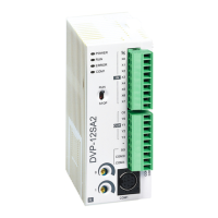
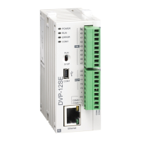
DVP12SE11R DVP12SE11T
Noise immunity
ESD (IEC 61131-2, IEC 61000-4-2): 8kV Air Discharge
EFT (IEC 61131-2, IEC 61000-4-4): Power Line: 2kV, Digital I/O: 1kV,
Analog & Communication I/O: 1kV
RS (IEC 61131-2, IEC 61000-4-3): 26MHz ~ 1GHz, 10V/m
Grounding
The diameter of grounding wire cannot be smaller than the wire
diameter of terminals L and N (All DVP units should be grounded
directly to the ground pole).
Operation / storage
Operation: 0 to 55°C (temp.), 50 to 95% (humidity), Pollution degree 2
Storage: -25 to 70°C (temp.), 5 to 95% (humidity)
Vibration / shock
resistance
International standards: IEC61131-2, IEC 68-2-6 (TEST
Fc)/IEC61131-2 & IEC 68-2-27 (TEST Ea)
Weight (g) 145 135
Input Points Spec.
Items
24 VDC (-15 to 20%) single common port input
Input No. X0 to X2 X3 to X7
Input type DC (SINK or SOURCE)
Input current (±10%) 24 VDC, 5 mA
Input impedance 4.7 kΩ
Max. frequency 100 kHz 10 kHz
Off On > 15 VDC Action
level
On Off < 5 VDC
Off On < 2.5 μs < 20 μs Response
time
On Off < 5 μs < 50 μs
Filter time Adjustable within 0 ~ 20ms by D1020 (Default: 10ms)
Output Points Spec.
Items
Relay Transistor
Output No. Y0 to Y3 Y0, Y2 Y1, Y3
Max. frequency 1 Hz 100 kHz 10 kHz
Working voltage 250 VAC, < 30 VDC
5 to 30 VDC
#1
Resistive 1.5 A/1 point (5 A/COM) 0.5 A/1 point (2 A/COM)
Inductive
#2
15 W (30 VDC)
Max. load
Lamp 20 WDC/100 WAC 2.5 W (30 VDC)
Off On
2 μs
#3
20 μs
#3
Response
time
On Off
Approx. 10 ms
3 μs
#3
30 μs
#3
#1: UP, ZP must work with external auxiliary power supply 24 VDC (-15 to +20%), rated
consumption approx. 1mA/point.
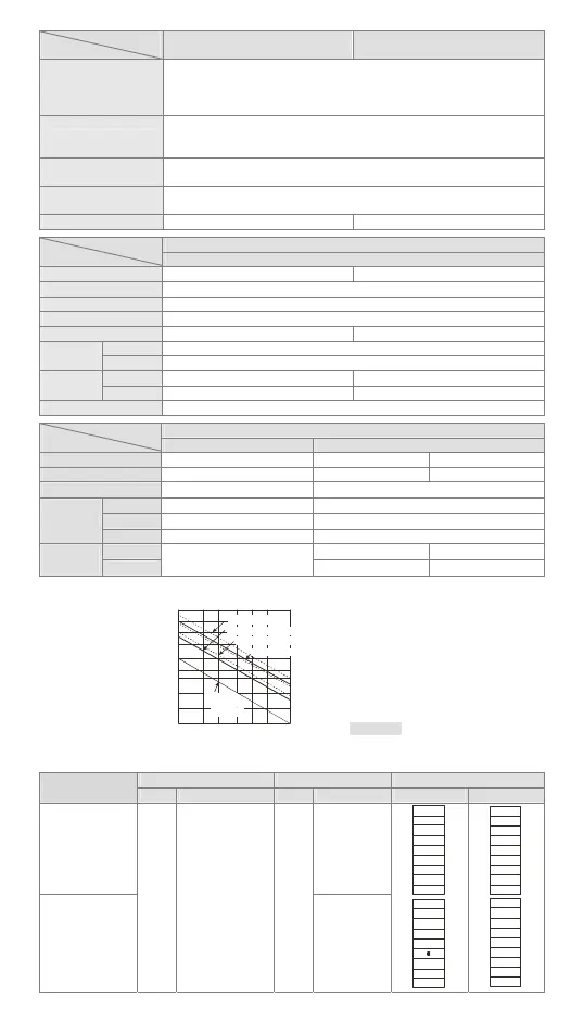
#2: Life curves
Contact
current(A)
0.5
0.1
0.2
50
0.3 0.7 1 2
200
300
500
100
1,000
2,000
3,000
O
p
e
r
a
t
i
o
n
(
X
1
0
)
3
120 VAC, resistive
30 VDC, inductive (t=7ms)
240 VAC, inductive (cos 0.4)
ψ
=
120 VAC, inductive (cos =0.4)
ψ
30 VDC,
inductive
(t=40ms)
[ Figure 2 ]
#3: Load = 0.5A
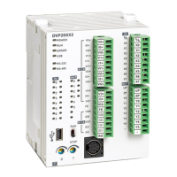
I/O Configuration
Input Output I/O Configuration
Model
Point Type Point Type Relay Transistor
DVP12SE11R Relay
DVP12SE11T
8
DC
(Sink Or Source)
4
Transistor
S/ S
X0
X1
X2
X5
X6
X7
Y0
Y1
Y2
SG
COM3+
COM3-
X4
C0
Y3
X3
S/ S
X0
X1
X2
X5
X6
X7
Y1
Y2
Y3
SG
COM3+
COM3-
X4
Y0
UP
X3
ZP
 Loading...