Do you have a question about the Denon Professional DN-F300 and is the answer not in the manual?
Procedure for checking leakage current before unit return.
General cautions for safe servicing, handling, and disassembly.
Guidance on replacing critical safety components with designated parts.
Troubleshooting steps for power-related issues.
Troubleshooting steps for display or control unit problems.
Troubleshooting steps for key operation failures.
Troubleshooting steps for audio/picture output issues.
Datasheet details for the UDA1345TS/N2 audio codec IC.
Datasheet details for the PCM1716E DAC converter IC.
Block diagram for the MC9508AW60 microcontroller.
Block diagram for the ST7066-0B LCD driver IC.
Block diagram for the ADSP-BF532 DSP processor.
Block diagram for the ADSP-BF532 DSP memory interface.
Block diagram for the ISP1761BE USB interface IC.
Component layout for the Input/Output Printed Wiring Board.
Component layout for the USB Printed Wiring Board.
Component layout for the Power Switch Printed Wiring Board.
Component layout for the SD Card Printed Wiring Board.
Component layout for the Control Printed Wiring Board.
Component layout for the Jack Printed Wiring Board.
Component layout for the Volume/Rotary control Printed Wiring Board.
Detailed parts breakdown for the I/O PCB.
Detailed parts breakdown for the Control PCB.
Detailed parts breakdown for the USB PCB.
Detailed parts breakdown for the Power Switch PCB.
Detailed parts breakdown for the SD Card PCB.
Detailed parts breakdown for the Jack PCB.
Detailed parts breakdown for the VFD PCB.
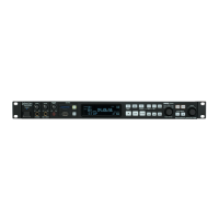
| Brand | Denon Professional |
|---|---|
| Model | DN-F300 |
| Category | Turntable |
| Language | English |