D-MASDV/D-MX7700DV
37
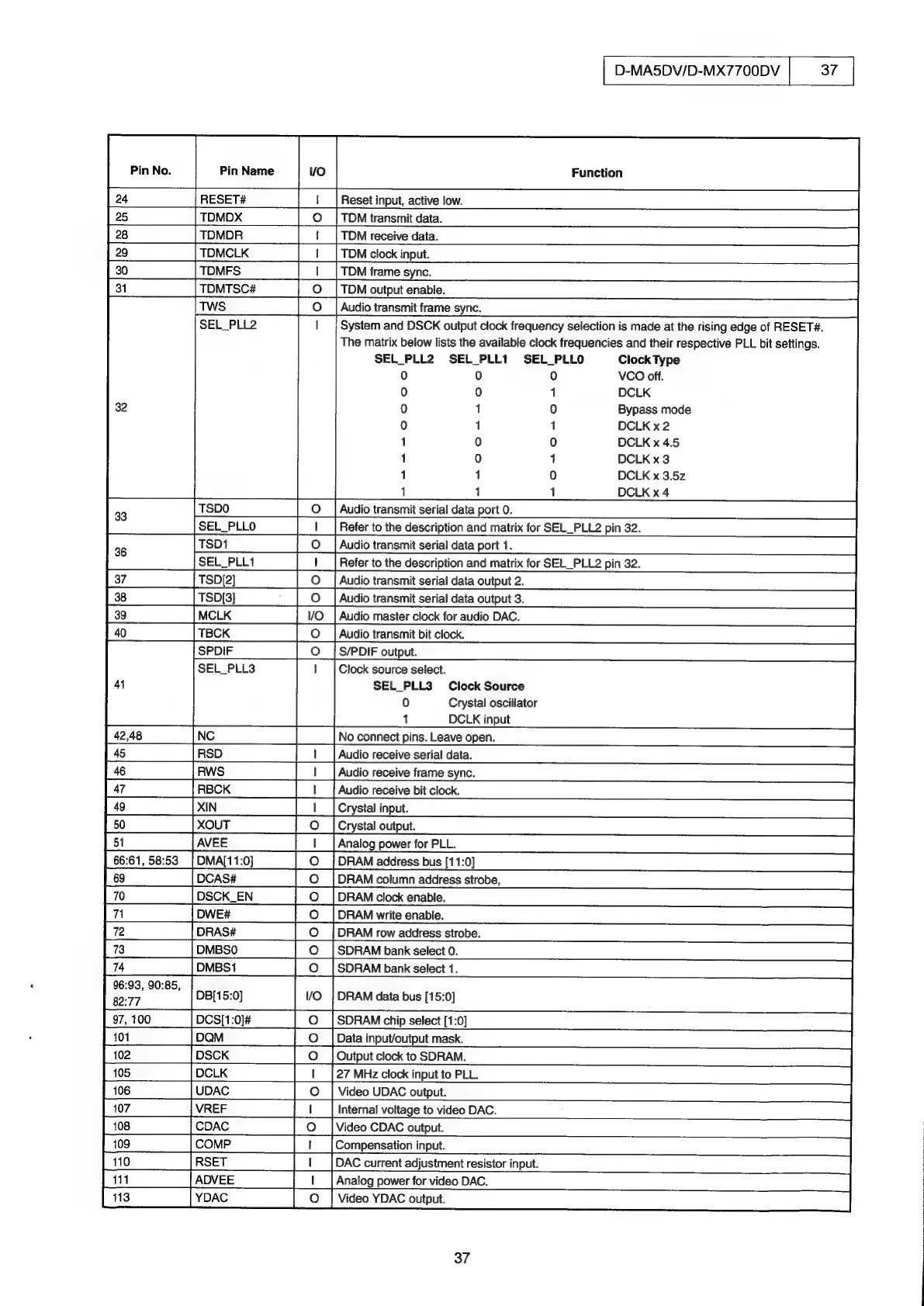
Reset
input,
active
low.
TDM
transmit
data.
TDM
receive
data.
TDM
clock
input.
Pin
Name
RESET#
TDMDX
TDOMDR
TDMCLK
TDMFS
TDMTSC#
Ss
SEL_PLL2
TDM
frame
sync
TDM
output
enable.
Audio
transmit
frame
sync.
System
and
DSCK
output
clock
frequency
selection
is
made
at
the
rising
edge
of
RESET#.
The
matrix
below
lists
the
available
clock
frequencies
and
their
respective
PLL
bit
settings.
SEL_PLL2
SEL_PLL1
SEL_PLLO
Clock
Type
30
wo
wo
N]M
1M
]
rw
ie)
=
O(oOjalr
0 0
0
VCO
off.
0 0
1
DCLK
0
1
0
Bypass
mode
0
1
1
DCLK
x
2
1
0
0
DCLK
x
4.5
1
0
1
DCLK
x
3
1
1
0
DCLK
x
3.5z
1 1
DCLK
x
4
1
sof
ESBo__|_
{ui
ens
seri
dataport.
[SEL_PLLO
|
_1_[Refertothe
description
and
matrixforSEL_PLL2pin32.
CS
jee
fESPL__f_
{Alo
ans
serial
dataport,
|SEL_PLL1
[|__|
Referto
the
description
and
matrixforSEL_PLU2pin32.SSC=d
[s7_
[tsp]
|
O
[Audiotransmitserialdataoutput2,
C—C“‘“‘“CS*S™S~*”
[38
[SDs]
|
[Audiotransmitserialdataoutput3.
SC~C~C~szY
[39
[CLK
|
VO
[Audio
masterclockforaudioDAC.C“‘“‘C™SCOC*C*#*#C#C#‘*C
140
=)
6
([tBCK.C‘C‘idCYS
Audio
transmit
bit
clock.
p
SEL_PLL3
Clock
source
select.
41
SEL_PLL3
Clock
Source
0
Crystal
oscillator
1
DCLK
input
No
connect
pins.
Leave
open.
45
[RSD
—S
|] it
|
Audio
receive
serial
data.
js
RWS
|
[Audioreceivetramesyne
j47_
ss
tRBCK
|
I
[Audioreceivebitciock,
CS
pao
xin,
|
[Grystabinput.
CS
ps0
fxour
|
[Crystaoutput
CS
psi
AVEE
|
[AnalogpowerforPLL,
Cd
|
66:61,58:53
|DMA[11:0]
|
O
|DRAMaddessbus
[11:0]
Cid
}6o_s|ocas#
|
©
[DRAMcolumnaddressstrobe,
CS
|70_s|DScKEN
|
O
[DRAMciockenable,
[71
fDwe#
|
O
[DRAMwriteenable,
CS
j72_s[pRaS#
|
©
|
DRAMrowaddressstrobe,
Cd
}73__spmeso_
|
©
[SDRAMbankselecto.
CS
[74_sjomest
|
O
[SDRAMbankselectt,
Cid”
96:93,
90:85,
DB[15:0]
DRAM
data
bus
[15:0]
197,100
_-[Dcsit:o#
——|_O_|
SDRAM
chip
select
[1:0]
pio
}DaM
|
[Datainputioutputmask
CS
jw2
i
fosck
|
O
[OutputclocktoSDRAM
Cd
fs
DcLK
tf
27
MHz
clock
inputtoPLL
TT
C~—~sdY
p06
fupac
|
[Video
uDAC
output
CC—“—sCSCSCsdS
[107
s|VREF
|
1
[InternalvoltagetovideoDAG.
CSCi*”
[ios_fcbac
|
[VideoCDaC
output,
C—~—“C~™SCSC*dS
j09_
i
}comp
||
[Compensationinput
Te
CCSC~C‘*dS
Piio—=F~S—«iéd(RSeTtC“‘C‘“‘dL'YSCd’'
DAC
current
adjustment
resistor
input.
i1-sdfADveE—~—~sSsC
CS
Analog
power
for
video
DAC.
113
YDAC
[|Video
YDAC
output
COC~—SC“‘S*‘“‘S*~*Y
37
 Loading...