EasyManua.ls Logo

Digilent Basys 2 - Built-In Self Test

Digilent Basys 2
12 pages
Print Icon
To Next Page IconTo Next Page
To Previous Page IconTo Previous Page
Loading...
Copyright Digilent, Inc. All rights reserved.
Other product and company names mentioned may be trademarks of their respective owners.
Page 11 of 12
8 FPGA Pin Definitions
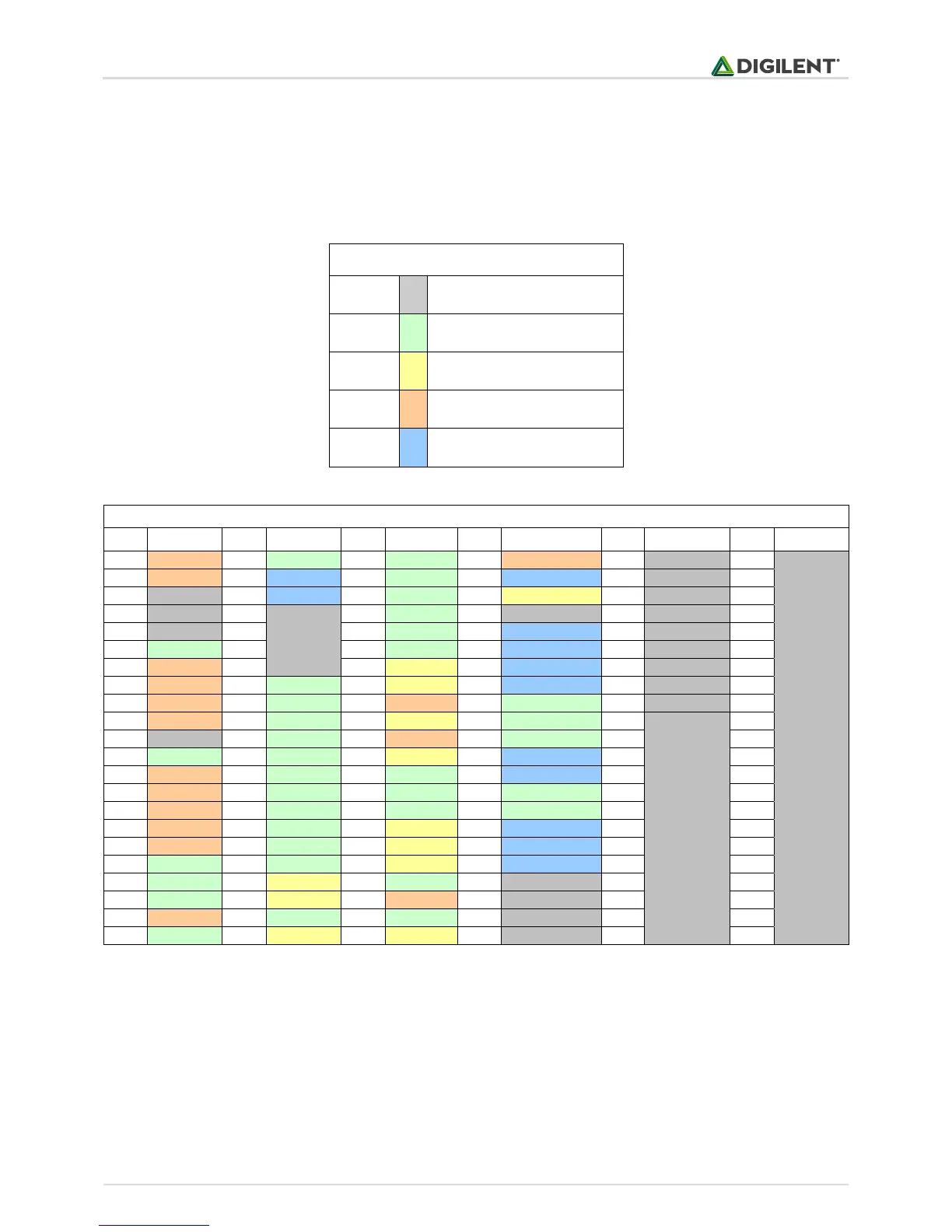
The table below shows all pin definitions for the Spartan-3E on the Basys 2 board. Pins in grey boxes are not
available to the user.
FPGA pin definition table color key
Grey
Not available to user
Green
User I/O devices
Yellow
Data ports
Tan
Pmod port signals
Blue
USB signals
Basys 2 Spartan-3E pin definitions
Pin
Signal
Pin
Signal
Pin
Signal
Pin
Signal
Pin
Signal
Pin
Signal
C12
JD1
P11
SW0
N14
CC
B2
JA1
P8
MODE0
M7
GND
A13
JD2
M2
USB-DB1
N13
DP
C2
USB-WRITE
N7
MODE1
P5
GND
A12
NC
N2
USB-DB0
M13
AN2
C3
PS2D
N6
MODE2
P10
GND
B12
NC
M9
NC
M12
CG
D1
NC
N12
CCLK
P14
GND
B11
NC
N9
NC
L14
CA
D2
USB-WAIT
P13
DONE
A6
VDDO-3
C11
BTN1
M10
NC
L13
CF
L2
USB-DB4
A1
PROG
B10
VDDO-3
C6
JB1
N10
NC
F13
RED2
L1
USB-DB3
N8
DIN
E13
VDDO-3
B6
JB2
M11
LD1
F14
GRN0
M1
USB-DB2
N1
INIT
M14
VDDO-3
C5
JB3
N11
CD
D12
JD4
L3
SW1
P1
NC
P3
VDDO-3
B5
JA4
P12
CE
D13
RED1
E2
SW6
B3
GND
M8
VDDO-3
C4
NC
N3
SW7
C13
JD3
F3
SW5
A4
GND
E1
VDDO-3
B4
SW3
M6
UCLK
C14
RED0
F2
USB-ASTB
A8
GND
J2
VDDO-3
A3
JA2
P6
LD3
G12
BTN0
F1
USB-DSTB
C1
GND
A5
VDDO-2
A10
JC3
P7
LD2
K14
AN3
G1
LD7
C7
GND
E12
VDDO-2
C9
JC4
M4
BTN2
J12
AN1
G3
SW4
C10
GND
K1
VDDO-2
B9
JC2
N4
LD5
J13
BLU2
H1
USB-DB6
E3
GND
P9
VDDO-2
A9
JC1
M5
LD0
J14
HSYNC
H2
USB-DB5
E14
GND
A11
VDDO-1
B8
MCLK
N5
LD4
H13
BLU1
H3
USB-DB7
G2
GND
D3
VDDO-1
C8
RCCLK
G14
GRN2
H12
CB
B14
TMS
H14
GND
D14
VDDO-1
A7
BTN3
G13
GRN1
J3
JA3
B13
TCK-FPGA
J1
GND
K2
VDDO-1
B7
JB4
F12
AN0
K3
SW2
A2
TDO-USB
K12
GND
L12
VDDO-1
P4
LD6
K13
VSYNC
B1
PS2C
A14
TDO-S3
M3
GND
P2
VDDO-1
9 Built-In Self Test
The Basys 2 board comes preloaded with a simple self test/demonstration project stored in its ROM. The demo
project (available at the website) shows how the Xilinx CAD tools connect FPGA signals to Basys 2 circuits. Since the
project is stored in ROM, it can also be used to check board functions. To run the demo, set the ROM/USB jumper
(JP3) to ROM and apply power to the board; the seven-segment display will show counting digits, the switches will
turn on individual LEDs, the buttons will turn off individual digits on the seven segment display, and a test pattern
is driven on the VGA port.