Do you have a question about the Digital Equipment pdp11 and is the answer not in the manual?
Explains how peripherals are programmed using memory reference instructions and device registers.
Details the two types of registers associated with each device: control/status and data registers.
Describes the general form and typical bit assignments in control and status registers for peripherals.
Introduces basic PDP-11 I/O devices: teleprinters, paper tape units, line printers, and card readers.
Describes the ASR 33 Teletype, its operation, programming, registers, and specifications.
Details the LP11 high-speed line printer, its operation, programming, and specifications.
Explains the CR11 and CM11 card readers, their operation, programming, and specifications.
Describes the DECtape TC11/TU56 dual-transport system, its introduction, operation, and programming.
Details the TM11/TU10 magnetic tape system, its introduction, operation, and programming.
Describes the VT01A storage display unit, its specifications, and operation.
Details the VR01A oscilloscope, its specifications, and applications.
Explains the VR14 point plot display, its specifications, and features.
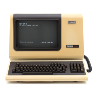
Describes the VT05 alphanumeric display terminal, its specifications, and capabilities.
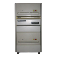
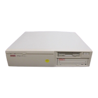
Discusses various mass storage alternatives available for PDP-11 users, including fixed-head and moving-head systems.
Details the RC11/RS64 disk memory system, its introduction, operation, and programming.
Explains the RF11/RS11 disk and control system, its introduction, operation, and programming.
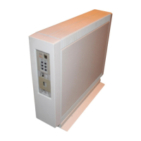
Describes the DECpack cartridge disk system, its introduction, operation, and programming.
Details the KW11-P programmable real time clock, its introduction, operating modes, and programming.
Explains the KW11-L line time clock, its programming, and specifications.
Introduces UNIBUS extension options like bus extenders and bus switches for PDP-11 systems.
Details the DT11-A and DT11-B bus switches, their operation, switch positions, and control.
Overview of DIGITAL's interfaces for PDP-11 communications applications.
Describes the DC11 series interface for serial asynchronous lines, its operation, and programming.
Explains the DN11 ACU interface for dialing telephone numbers and establishing data links.
Details the DP11 synchronous line interface, its operation, and specifications.
Describes the DM11 multiplexer, its introduction, operation, programming, and specifications.
Explains the KL11 interface for full duplex asynchronous serial lines, its programming, and specifications.
Details the H312A null modem for connecting terminals to computers without modems.
Describes the AFC11 analog input subsystem for industrial data acquisition.
Details the AD01-D subsystem for multichannel analog data acquisition.
Explains the AA11-D subsystem for multichannel digital to analog conversion.
Describes the UDC11 for industrial digital I/O, its operation, and modules.
Details the PDP-11 UNIBUS signal lines, bus transactions, timing, and interfacing.
Explains the bidirectional and unidirectional lines used for data transfer on the UNIBUS.
Describes the 16 data lines used to transfer information between master and slave devices.
Explains the 18 address lines used by the master device to select a slave device or memory location.
Details the control signals for data transfer operations, master/slave synchronization, and parity checking.
Describes the UNIBUS priority transfer lines, including bus request and grant lines.
Explains bus activity, interlocking of control signals, and asynchronous data transfer.
Details bus control transfer based on priority arbitration logic and device chaining.
Discusses UNIBUS timing restrictions, signal transmission, and delays for data transfer.
Explains PDP-11 address mapping, reserved locations for traps, interrupts, and device registers.
Discusses UNIBUS transmission, signal levels, length, and receiver/transmitter circuits.
Describes UNIBUS cable types, impedance, and transmission characteristics.
Explains the standard UNIBUS signal levels and terminology for active states.
Details UNIBUS length limitations and loading constraints, including repeater options.
Shows equivalent circuits for UNIBUS receivers and transmitters and their characteristics.
Describes modules used for UNIBUS interfacing: jumper module, cable, transmitters, and receivers.
Details UNIBUS jumper modules and Flexprint cable assemblies.
Explains the M930 UNIBUS Terminator Module for signal line termination.
Discusses UNIBUS driver and receiver modules (M783, M784, M785, M798).
Details the M105 Address Selector Module for selecting device registers and controlling bus signals.
Describes the M7820 module for making bus requests and generating interrupts.
Explains the M7821 module as a replacement for M7820, improving system performance.
Details the M795 module for DMA devices, including counters for data transfers and bus addresses.
Describes the M796 module for controlling data transfer operations as a UNIBUS bus master.
Provides a description of hardware designed for PDP-11 system interfacing.
Details the BB11 Blank Mounting Panel for general interfacing and system unit mounting.
Explains the DD11-A panel for mounting small peripheral interfaces.
Describes the simplest read/write interface using a storage register and bus gating circuits.
Explains a programmed interface for analog-to-digital converters (ADC).
Details an interface with interrupt capability for ADC, allowing concurrent execution.
Describes the DMA interface for data transfers between devices and memory without processor intervention.
Provides an output interface with interrupt control for DAC devices.
Details the DAC-DMA interface for transferring data directly from memory to DAC.
Presents an interface between PDP-11 UNIBUS and another computer's data channel.
Describes the interface for PDP-11 to PDP-11 communication, enabling processor interaction.
Explains the DR11-B DMA interface for direct data transfers between UNIBUS and user devices.
Lists interrupt vector addresses and their corresponding devices or functions.
Provides a list of device registers and their assigned UNIBUS addresses.
Details UNIBUS pin assignments based on pin numbers.
Lists UNIBUS pin assignments based on signal names.
Provides BB11 power pin assignments for system units.
| Brand | Digital Equipment |
|---|---|
| Model | pdp11 |
| Category | Desktop |
| Language | English |