Do you have a question about the DTK PIM-TB10-Z and is the answer not in the manual?
Provides an introduction to the motherboard and its key features for personal computers.
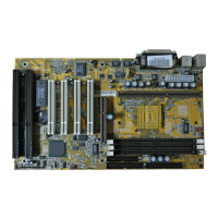
Illustrates the physical layout of the PIM-TB10-Z motherboard and its onboard jumpers.
Details the location of RAM banks and proper chip insertion for system memory.
Explains installation of ROM chips (BIOS, BASIC) in specified sockets.
Provides a table for configuring RAM size and notes on chip usage in banks 2 and 3.
Details settings for operation modes, coprocessor, and graphics adapters using DIP switch SW1.
Clarifies the meaning of "ON" and "OFF" states for DIP switch settings.
Discusses motherboard mounting in various system unit cases and optional panel displays.
Describes the keylock connector's role in controlling the keyboard lock/unlock status.
Details reset connector (JP4) and pinouts for Power LED/Turbo LED (JP5).
Explains hardware switch (JP6) for mode selection and speaker connector (JP1) pinouts.
Details the 12-pin power supply connector (P1) pinout.
Details the 5-pin DIN keyboard connector pin assignments for clock, data, and power.
Explains using plastic and brass connectors for secure motherboard mounting and grounding.
Emphasizes turning off power before any hardware changes to ensure system reliability.
Introduces the motherboard's dual clock system (4.77MHz/10MHz) for improved computing speed.
Guides on setting the default operation mode (Normal/Turbo) using jumper JP6.
Explains using keyboard shortcuts to switch between Turbo and Normal modes.
Describes using a physical hardware switch to select Turbo or Normal mode.
Discusses software operation in Turbo mode, noting potential issues with specific applications.
Provides a general technical overview of the system board, its components, and expansion slots.
Details the 8088 processor, clock speeds, and support for coprocessors.
Explains the role of DMA channels for data transfers and timer counters for system timing.
Describes the system's eight interrupt levels and their prioritization for devices.
Covers ROM/EPROM and R/W memory support, capacities, and minimum requirements.
Details the keyboard interface, interrupt generation, and the 5-pin DIN connector.
Explains the speaker connection, power, and different methods for driving audio output.
Details the I/O channel's 8-bit data bus, 20 address lines, and interrupt structure.
Describes the OSC, CLK, and Reset signals essential for system operation.
Explains address (A0-A19) and data (D0-D7) bus signals.
Details ALE for latching addresses and I/O CH CK for parity error reporting.
Describes the I/O CH RDY signal for managing device readiness in I/O cycles.
Explains IOR, IOW, MEMR, MEMW command signals for device interaction.
Details DRQ and DACK lines for managing DMA requests and acknowledgments.
Explains AEN for DMA control and T/C for indicating DMA completion.
Covers CARD SLCTD signal and voltage availability on the I/O channel.
| Brand | DTK |
|---|---|
| Model | PIM-TB10-Z |
| Category | Motherboard |
| Language | English |