2 Schematic Checklist
5 4 3 2 1
D D
C C
The values of C1 and C2 vary with
the selection of the crystal.
The value of R1 varies with the actual
PCB board.
GPIO19
U0RXD
GPIO18
LNA_IN
GPIO0
GPIO1
SPICS0
SPID
SPIQ
SPICLK
SPIWP
RF_ANT
U0TXD
SPICS0 SPID
GND
VDD33
GNDGND GND
GND GND
VDD33
VDD_SPI
GND
GND
GND GND
C1
TBD
C9
TBD
R6 0
R1 0
ANT1
PCB_ANT
1
2
R5 0
C3
1uF
R2 499
R3 0
L1 2.0nH
C2
TBD
C8
TBD
C6
0.1uF
L2
TBD
C5
10uF
C4
10nF
C7
0.1uF
LNA_IN
1
VDD3P3
2
VDD3P3
3
XTAL_32K_P
4
20
SPICS0
21
SPICLK
22
SPID
23
SPIQ
24
U0RXD
27
U0TXD
28
XTAL_N
29
XTAL_P
30
GND
33
VDDA
32
VDDA
31
GPIO19
26
GPIO18
25
U1
40MHz(±10ppm)
XIN
1
GND
2
XOUT
3
GND
4
B B
A A
The values of C8, L2 and C9
vary with the actual PCB board.
If using ESP32-C3FN4 or ESP32-C3FH4,
external flash could be removed.
CHIP_EN
GPIO4
GPIO5
GPIO6
GPIO7
GPIO8
GPIO9
GPIO10
GPIO3
SPICLK
SPIHD SPIWP
SPIQ
XTAL_P
GND
GNDGND
GND GNDGND
VDD33
VDD_SPI
VDD33
GND
GND
VDD33
GND
VDD33
L3
TBD
U3 FLASH-3V3
C12
0.1uF
C10
0.1uF
R1 0
C1
10nF
Y1
40MHz(±10ppm)
VCC
4
NC
1
GND
2
OUT
3
R8
10K
C11
1uF
U2 ESP32-C3
CHIP_EN
7
MTMS
9
MTDI
10
VDD3P3_RTC
11
MTCK
12
MTDO
13
GPIO8
14
GPIO9
15
GPIO10
16
VDD3P3_CPU
17
VDD_SPI
18
SPIHD
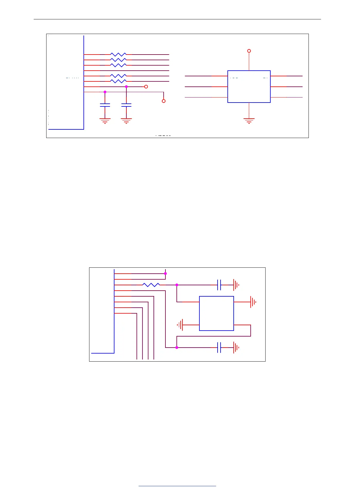
Figure 5: ESP32C3 Family Flash Circuit
2.4 Clock Source
There are two clock sources for ESP32-C3 family, namely an external crystal clock source and an RTC clock
source.
2.4.1 External Clock Source (compulsory)
Currently, the ESP32-C3 family firmware only supports 40 MHz crystal. The specific capacitance of C1 and C2
depends on further testing of, and adjustment to, the overall performance of the whole circuit. Please add a
component in series on the XTAL_P clock trace to reduce the drive capability of the crystal and to minimize the
impact of crystal harmonics on RF performance. The value of this component (initially of 24 nH) depends on
further testing. Note that the accuracy of the selected crystal needs to be ±10 ppm.
NC: No component.
The values of C8, L2 and C9
vary with the actual PCB board.
The values of C1 and C2 vary with
the selection of the crystal.
The value of R1 varies with the actual
PCB board.
GPIO19
CHIP_EN
GPIO4
GPIO5
GPIO6
GPIO7
GPIO8
U0RXD
GPIO18
LNA_IN
GPIO9
GPIO10
GPIO0
GPIO1
SPICS0
SPID
SPIQ
SPICLK
SPIWP
SPIHDGPIO2
GPIO3
RF_ANT
U0TXD
SPICLK
SPICS0
SPIHD SPIWP
SPID
SPIQ
GND
VDD33
GND
GND
GNDGND GND
GND GND
GND
VDD33
GND GNDGND
VDD33
VDD_SPI
VDD33
GND
VDD_SPI
GND
GND
GND GND
C1
TBD
C9
TBD
U3 FLASH-3V3
/CS
1
DO
2
/WP
3
GND
4
DI
5
CLK
6
/HOLD
7
VCC
8
R4 0
R7 0
R6 0
C12
0.1uF
R1 0
ANT1
PCB_ANT
1
2
R5 0
C10
0.1uF
C3
1uF
R2 499
R3 0
L1 2.0nH
C2
TBD
C8
TBD
C6
0.1uF
L2
TBD
C5
10uF
C4
100pF
C7
0.1uF
C11
1uF
U2 ESP32-C3
LNA_IN
1
VDD3P3
2
VDD3P3
3
XTAL_32K_P
4
XTAL_32K_N
5
GPIO2
6
CHIP_EN
7
MTMS
9
MTDI
10
VDD3P3_RTC
11
MTCK
12
MTDO
13
GPIO8
14
GPIO9
15
GPIO10
16
VDD3P3_CPU
17
VDD_SPI
18
SPIHD
19
SPIWP
20
SPICS0
21
SPICLK
22
SPID
23
SPIQ
24
U0RXD
27
U0TXD
28
XTAL_N
29
XTAL_P
30
GND
33
GPIO3
8
VDDA
32
VDDA
31
GPIO19
26
GPIO18
25
U1
40MHz(±10ppm)
XIN
1
GND
2
XOUT
3
GND
4
R8
10K
Figure 6: Schematic for ESP32C3 Family’s Crystal
Espressif Systems 9
Submit Documentation Feedback
ESP32-C3 Family Hardware Design Guidelines V1.0
 Loading...