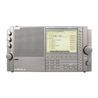
E1 THEORY OF OPERATION
RF BOARD
Please refer to the E1 Main Board Block Diagram (Figure 1) as you follow this description. References will also be
made to components shown on the “SCH. Main RF Board” schematic drawings 1 thru 6.
Power
Input
Default power is provided by the batteries if
installed. External power enters through J1 and CR36. A
contact in J1 detects if the jack has a plug installed, and
if so, produces the PWR_JACK signal for the front panel
board. If there is a plug installed, R284 passes a voltage
(EXT_PWR) to the front panel board in order to detect if
external power is actually present. CR36 prevents
voltage from backing out of the jack if batteries are
installed. Also, if batteries are installed, Q75 disconnects
them when external power is present to prevent them
from charging. R324 and Q21 control Q75 based on the
presence of external power. Q75 also provides reverse
battery polarity protection for the receiver. Power from
the batteries or an external power source passes
through a self resettable fuse (F1) to the V_BAT
connection.
Distribution
Q74 connects V_BAT to regulator U27 to turn the
receiver on. Q74 is controlled by the front panel board
through Q20. Voltage from Q27 is applied to Q72, Q71,
and Q70. Then, depending on mode (MODE_A,
MODE_B), the appropriate transistor is turned on via
Q16 through Q19 to provide power to the corresponding
circuitry.
Antenna Input
Signals from the LW, MW, SW (hereafter referred to
as HF) and FM bands enter the receiver from one of two
sources; the internal telescopic whip antenna (P4), or
the external antenna connector (J6). Neon bulb GL1
and resistor R322 at the EXT_ANTENNA input guard
against static buildup, and diodes CR17 through CR20
perform a similar function for the telescopic whip
antenna.
Signals from the internal telescopic whip antenna pass
through Q59 which buffer the high impedance signals
down to 50Ù, and are then applied to one pole of SW1
(the ANTENNA – HF switch) and of SW2 (the ANTENNA
– FM switch). Transistor Q15 turns Q59 on and off.
Signals from the EXT_ANTENNA connector J6 are
applied to the other pole of these two switches. Switch
SW1 selects which of these two signal sources is
connected to the HF section of the receiver, and SW2
selects which input is connected to the VHF (FM)
section.
HF Section
Signal Path
Signals intended for the HF section of the receiver
pass from switch SW1 through T4 which provides
impedance transformation from 50Ù to 450Ù. T4 feeds
the signals to the input of a bank of filters (one low pass
and 5 bandpass) which selectively cover the range of .1
MHz to 30 MHz. The filter which is selected at any given
time is determined by the frequency to which the
receiver is tuned. The actual switching is accomplished
by PIN diodes CR24 through CR35, transistors Q25
through Q30 and latch U21. (See schematic 1 of 6 for
these items.) Serial data applied to latch U21 from the
front panel board determines which of lines BP_A
through BP_F are pulled high. The line which is high
turns on one of transistors Q25 through Q30 which in
turn applies forward bias to the two PIN diodes for the
selected filter. The signals then pass through T5 which
transforms the impedance back down to 50Ù.
If the DX function is selected, the signal passes
through switching transistor Q33, and is amplified by
preamplifier transistor Q8. It then passes on through
switching transistor Q34 to the first mixer. If the DX
function is not selected, Q8 is bypassed by Q35 and the
signal is not amplified. Transistors Q400, Q401, and
Q402 control the preamp switching.
The signal then passes through a low pass filter with
a cutoff just above 30 MHz which prevents UHF ingress,
and is applied to a balanced mixer (1
st
HF Mixer),
consisting of Q63 and Q64, T6, T7, and T8. R452 is
used to adjust the balance of the mixer in order to
minimize any broadband noise present at the LO input
(45.1 – 75 MHz).
In the 1
st
HF Mixer, the desired signals are
combined with signals from the HF LO (Q2 and Q10) to
produce a first IF frequency of 45 MHz. The HF LO
operates over a frequency range of 45.1 to 75 MHz. The
45 MHz signals then pass through 45 MHz bandpass
filters CF3 and CF4 with a combined effective bandwidth
of 8 kHz and on through I.F. amplifier Q76, the gain of
which is controlled by AGC2. The output of Q76 is fed
through Q79 which buffers the signal to low impedance.
Q79 applies the signal, to the gate of 2
nd
Mixer Q65
where the signal is mixed with a 44.545 MHz signal from
Second LO consisting of oscillator transistor Q81, crystal
Y2, and buffer Q80. The 2
nd
LO signal is applied to the
 Loading...