22
22
2
INTRODUCTIONINTRODUCTION
INTRODUCTIONINTRODUCTION
INTRODUCTION
The Promega 3 is a complex instrument and to be repaired requires a detailed
knowledge especially on digital boards as 761257 - CPU & SOUNG GENERATOR BOARD
and 256+256Mb DUAL DRAKE SOUND BOARDs.
If you need to repair these parts by yourself we suggest to replace them entirely,
otherwise the following information can be useful to locate a specific problem.
FUNCTIONAL DESCRIPTIONFUNCTIONAL DESCRIPTION
FUNCTIONAL DESCRIPTIONFUNCTIONAL DESCRIPTION
FUNCTIONAL DESCRIPTION
The new keyboards 2000 series, of which PROMEGA 3 is the first keyboard developed
by GM, are designed around the new processor DRAKE (Dsp Risc Advanced Keyboard
Engine).
Inside PROMEGA3 5 DRAKE have assembled on, the first one on the main board and
the others are mounted on 2 sound boards.
The first DRAKE controls the general management, all the I/Os and the sound
processing (mixer and digital effects) while the others are used for sounds generation.
All sounds and operating system are stored inside NAND FLASH memories, the FLAH
memory content is decompressed and transferred in the SDRAM memories to allow fast
elaboration.
The decompression task requires about 1 minute, to avoid this time the SDRAMs have
been endowed of a battery supply circuit (+VBAT, +VBRAM); under normal conditions,
after 3/4 working hours, the batteries are completely re-charged and they allow the
data retention for over 1 week.
The numbers between parentheses are referred to the same points reported on the
schematic diagrams.
[1] MASTER RESET[1] MASTER RESET
[1] MASTER RESET[1] MASTER RESET
[1] MASTER RESET
Starting from the switch ON event the keyboard remains in reset condition; when the
5V supply rail reaches about 4.75V IC35 (MAX709) set high the VOK after 200mS,
which enters in the DRAKE pin 209; the RST is delayed of further 100uS respect VOK
and it goes in the DRAKE pin 161, it is synchronized to the PLL internally, goes out
through pin 213 and enters in pin 206 of the same DRAKE; besides it is also sent to the
same pins of each DRAKE connected by the SLOT BUS, in this way all DSP are
synchronized.
The RST is also sent to other ICs to initialize the I/O circuitry, see also the schematics
and timing table.
[2] MASTER CLOCK[2] MASTER CLOCK
[2] MASTER CLOCK[2] MASTER CLOCK
[2] MASTER CLOCK
The Master clock (MCLK) produced by the oscillator XT1 (11.2896MHz) is sent through
IC31 and IC26 (DS90 LVDS Low voltage differential signaling) to each DRAKE, DAC, ADC
and expansion SLOT. The LVDS receivers placed at each termination of the balanced
signal (REFCLK) are used to get a perfect synchronism between all the devices.
By means of IC25 (74lvc74) also the sample frequency FS (44.1KHz), deriving from
IC54 (ADCL/RCLK) or from a SLOT (EX_FS), is synchronized with MCLK.
[3] START UP SETTING[3] START UP SETTING
[3] START UP SETTING[3] START UP SETTING
[3] START UP SETTING
During the rising slope of RST, DRAKE configure
itself reading the state of address pins between
AD0...AD30-A and A0...A2-D, if the configuration
doesn’t match to a valid one, a malfunction could
happen.
Check these in the CPU and SOUND BOARD sche-
matics.
[4] BOOTSTRAP[4] BOOTSTRAP
[4] BOOTSTRAP[4] BOOTSTRAP
[4] BOOTSTRAP
The jumper J1 can be set on two positions:
UART = The DRAKE bootstrap happens from the
COMPUTER serial port.
E
2
= The DRAKE bootstrap happens from the
eeprom device (IC15).
Initially, when the eeprom is empty, this jumper
must be set on UART, after the bootstrap is uploaded
into eeprom, the jumper J1 must be set to E
2
.
N.B. The 761257 spare parts already have the
bootstrap installed into eeprom.
[5] OPERATING SYSTEM & WAVE MEMORY[5] OPERATING SYSTEM & WAVE MEMORY
[5] OPERATING SYSTEM & WAVE MEMORY[5] OPERATING SYSTEM & WAVE MEMORY
[5] OPERATING SYSTEM & WAVE MEMORY
Often it happens that a malfunction of the instru-
ment is to investigate between the software rather
than the hardware.
Consequently it is necessary to know which Oper-
ating System (OS) version is loaded in the instru-
ment and eventually upgrade it with the last one
available; if the malfunction persists even if the
instrument is upgraded, please send a detailed
report to GM Italy.
The OS is contained in the NAND FLASH (IC7 and CN1) devices; these memories are
managed in similar way of a hard disk, for this reason GM supplies as spare part 761257
(CPU BOARD) including 761235 (NAND FLASH MODULE).
As discussed above to speed up the instrument OS and Waves are transferred on
SDRAM memory at the first startup, and are maintained on it by means of an internal
battery; till the battery is charged, or you does not force a restore as described further,
OS and waves are maintained on SDRAM.
To load for the first time or to upgrade with the last OS release, you need the
‘O.S.UPGRADE CD-ROM’ that is sent from GM upon request.
When you ask it please note your instrument serial number (SN#), it is written on the
label applied on the instrument backside, please also check the OS version and notify
both these information with the request.
To check the OS version proceed as follows:
Press the SPLIT P. button and, holding it down, press the “+” key at the side of the LCD:
on display appears the OS version number and date. Pressing again the “+” button the
display will show the filenames loaded into the instrument.
The OS version contained in the CD is specified by suffix in the filename (e.g.
Upgrade_PROMEGA3_v.1.01.exe); obviously, if the version installed on the instrument
is the same, the upgrade is not required.
IMPORTANT: When an instrument OS is upgraded, or when you want to restore the
initial manufacturer OS from NAND FLASH into SDRAM memories, you must press the
STANDBY button and, holding it down, turn on the instrument from the main
power switch. Firstly the display shows the result of the DRAM memory checksum
(WCKS OK or WCKS BD) secondly the state of the battery charge (BATT OK Or BATT
BD), where OK means good and BD means BAD; then the instrument will continue
forcing the decompression in the DRAM that requires about 1 min.; finally 5 OK will be
visualized to confirm the correct memorization on the SDRAMs of each DRAKE.
[6] RAM BACKUP & POT’S MOTORS SUPPLY RAIL[6] RAM BACKUP & POT’S MOTORS SUPPLY RAIL
[6] RAM BACKUP & POT’S MOTORS SUPPLY RAIL[6] RAM BACKUP & POT’S MOTORS SUPPLY RAIL
[6] RAM BACKUP & POT’S MOTORS SUPPLY RAIL
The board 731050-POT MOTOR SUPPLY & STAND-BY BOARD handles the supply rail of
the motorized potentiometers and, at the same time, the battery recharge; however
the 731011 - SWITCHING SUPPLY UNIT doesn’t have enough current for both circuit
simultaneously, two current limiters are connected in series (TR2, TR5 and TR3, TR4),
that privilege the motors supply (IC4) on request instead the recharging of the battery
(IC2).
IC1 inhibit the complete discharge of the batteries to extend their life, IC3 stabilizes
the 3.3V supply rail for the SDRAMs and TR1, by means of an impulse from the CPU,
handles to re-start the recharge circuitry every around 15min. and each time that the
state of the batteries charge is checked by CPU.
[7] SOUND BOARD (SLOT), PEDALS, AU-[7] SOUND BOARD (SLOT), PEDALS, AU-
[7] SOUND BOARD (SLOT), PEDALS, AU-[7] SOUND BOARD (SLOT), PEDALS, AU-
[7] SOUND BOARD (SLOT), PEDALS, AU-
DIO, PANEL checks using TESTMON tool.DIO, PANEL checks using TESTMON tool.
DIO, PANEL checks using TESTMON tool.DIO, PANEL checks using TESTMON tool.
DIO, PANEL checks using TESTMON tool.
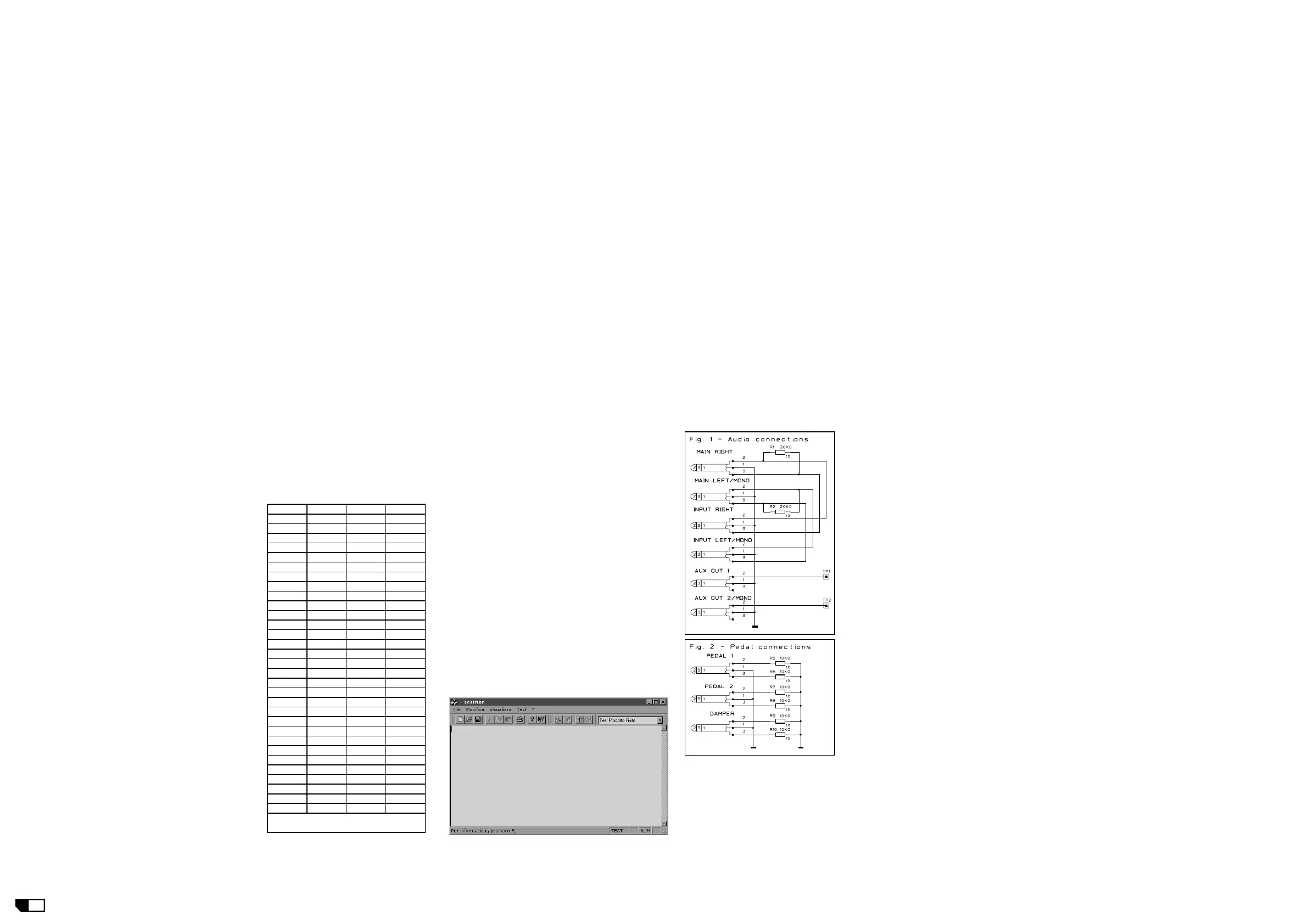
To perform these tests you must have a PC (Windows
95 or more) and the TESTMON program with the
follows precautions:
• A suitable serial cable (GM code 130429) is re-
quired.
• A suitable hardware (not provided) is necessary,
see schematic figures 1 and 2.
• A complete re-loading of OS is necessary after
using this program.
• The TESTMON program can be request to GM Italy
only.
• The TESTMON program must be used only in the
form specified here, other functional test without
the suitable hardware (not provided) could com-
promise the CPU BOARD.
Proceed as follows:
1) Connect the PC serial port COMx to the instrument
COMPUTER port by means of the suitable cable.
Both apparatus must be switched OFF.
2) Turn on the PC install and run the TESTMOM
program, the following window appears on PC
screen:
3) Set the right COMx through the
“Test/Serial port” menu.
4) Turn on the instrument and the
test will start automatically visu-
alizing:
Name of test and current date:
________________ Test 4, today, time ________________
The sound modules first test will start:
- [9] Testing Ext. Modules (CN2, 6, 7, 8) :
Test result:
————————————— SCREENING —————————————
Chip_0 (IC4) Chip_1 (IC19)
Slot_0 (CN8) No No
Slot_1 (CN7) Yes Yes
Slot_2 (CN6) Yes Yes
Slot_3 (CN2) No No
Testing VOK —> OK
Testing BID —> OK
- Pass!
The pedal inputs second test will start:
- [11] Testing Pedal Inputs :
Test result:
- Pass!
The audio I/O third test will start:
- [12] Testing Audio Loop :
Verify that AUX OUT signals respect the specifications.
Verify, using an oscilloscope, that a sinusoidal signal of about 5Vpp is present on every
output.
The controls panel fourth test will start:
- [20] Testing Panel :
Use the controls on the instrument to perform the test
and verify on the display the reading values.
The panel test doesn’t send messages on this window, with
the exception of last test that signals the end of all
test.
Press STAND-BY to advance the test of a step:
- Step 1/15 lights on all the leds of the panel.
- Step 2/15 lights off all the leds of the panel.
- Steps 3/15 to 12/15 the digits vary from 0 to 9 and a led couple of each encoder flows.
- Step 13/15 the digits return to 0 and the display shows:
“Pi =... Mo =... Vo =... In =...”
Operating the Pitch, Modulation, Volume and Input controls from minimum to maximum
excursion verify that the reading values vary accordingly from 0 to 127.
Pressing each button on the panel the correspondent led lights on or causes a variation
on the nearest digits and finally that rotating the encoders, the leds of the correspond-
ing wheel light on in the same sense of rotation.
- Step 14/15 the display shows:
“AT =... Ct =... PC =...”;
Pressing the note keys beyond the end stroke the aftertouch value (AT) varies from a
minimum of 0 to a maximum of 127.
N.B. it is possible to set the AT by means of VR1 on the CPU BOARD, with the purpose
to get the optimum variation with the wishes pressure, in any case this setting always
remains subjective for 2 reasons: the first one is that being the strip in conductive
rubber the same one for all the keys, you can feel notably changes if a single note or
an accord is pressed, besides in the PROMEGA 3 the preset sounds that make possible
to set the AT are BRASS1 and BRASS2.
- Step 15/15 verifies the uniform motion of the motorized potentiometers.
- *********** TEST PASSED ***********
End of the test, switch off and on again the instrument.
Bit Bus Si
nal Resistor Initial State
0D16R391
1D17R450
2A2R230
3A3R280
4A4R240
5A5R250
6A6R260
7A7R270
8A8R351
9A9R401
10 A10 AR22 0
11 A11 AR22 1
12 A12 AR22 0
13 A13 AR22 0
14 D18 R37 1
15 D19 R78 1
16 D20 R38 0
17 D21 AR45 0
18 D22 AR45 0
19 D23 AR45 0
20 D24 R52 0
21 D25 R59 0
22 D26 R51 1
23 D27 R65 0
24 D28 R67 0
25 D29 R68 0
26 D30 AR45 0
27 DD16 AR37 0
28 DD17 AR37 1
29 DSPA2 AR37 0
30 DSPA3 AR37 0
* this chart is referred to 761257 only,
for 761229 refer to schematic only.
 Loading...