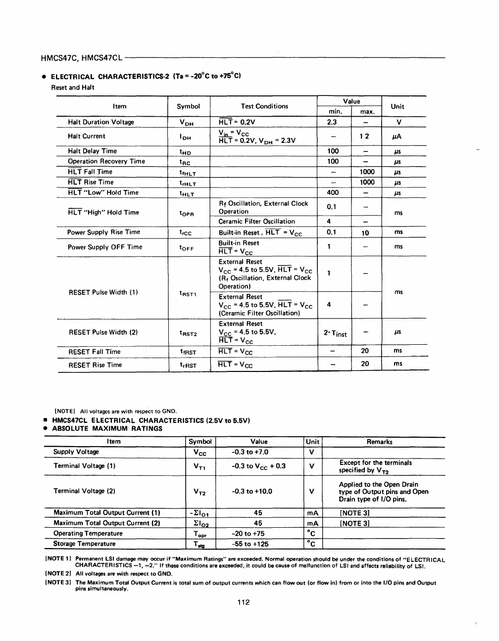
HMCS47C,HMCS47CL--------------------------------------------------------
• ELECTRICAL CHARACTERISTICS-2 (Ta = _20°C
to
+75°C)
Reset and Halt
Item Symbol Test Conditions
Halt Duration Voltage V
OH
HLT= 0.2V
Halt Current
IOH
~=Vee
HL
T = 0.2V, V
OH
= 2.3V
Halt Delay Time
tHO
Operation Recovery Time
tRe
HLT
Fall
Time
tfHLT
HL
T
Rise
Time
trHLT
HL
T
"Low"
Hold Time
tHLT
Rf
Oscillation, External Clock
HL
T "High" Hold Time
tOPR
Operation
Ceramic Filter Oscillation
Power Supply
Rise
Time
tree
Built-in Reset,
HL
T
=
Vee
Power Supply OFF Time
tOFF
Built-in Reset
HL
T =
Vee
External Reset
Vee = 4.5
to
5.5V,
HL
T = Vee
(Rf Oscillation, External Clock
RESET Pulse Width
(1)
Operation)
tRST1
External Reset
Vee = 4.5
to
5.5V, HLT = Vee
(Ceramic Filter Oscillation)
External Reset
RESET Pulse Width
(2)
tRST2
Vee
= 4.5
to
5.5V,
HLT =
Vee
RESET
Fall
Time
tfRST
HLT
=
VCC
RESET
Rise
Time trRsT
HLT=Vcc
[NOTE)
All
voltages
are
with
respe~t
to
GND.
•
HMCS47CL
ELECTRICAL CHARACTERISTICS (2.5V
to
5.5V)
• ABSOLUTE
MAXIMUM
RATINGS
Item Symbol
Value
Unit
Supply Voltage
Vee
-0.3
to
+7.0
V
Terminal Voltage
(1)
Vn
-0.3
to
Vee
+ 0.3 V
Terminal Voltage
(2)
V
T2
-0.3
to
+10.0
V
Maximum Total Output Current
(1)
-I:lo1
45
mA
Maximum Total
Output Current (2)
I:lo2
45
mA
Operating Temperature
Topr
-20
to
+75
°c
Storage Temperature
Tstg
-55
to
+125
°c
Value
min.
Unit
max.
2.3 - V
- 1 2
IlA
100
-
Ils
100 -
Ils
- 1000
IlS
-
1000
IlS
400
-
IlS
0.1
-
ms
4
-
0.1
10
ms
1 -
ms
1 -
ms
4
-
2·
Tinst
-
IlS
-
20
ms
-
20
ms
Remarks
Except for the terminals
specified
by
V
T2
Applied
to
the Open Drain
type of Output pins and Open
Drain type
of
I/O pins.
[NOTE 3)
[NOTE 3)
[NOTE
1)
Permanent
LSI
damage
may
occur
if
"Maximum
Ratings"
are
exceeded.
Normal
operation
should
be
under
the
conditions
of
"ELECTRICAL
CHARACTERISTICS
-1,
-2."
If
these
conditions
are
exceeded,
it
could
be
cause
of
malfunction
of
LSI
and
affects
reliability
of
LSI.
[NOTE
21
All
voltages
are
with
respect
to
GND.
[NOTE
31
The
Maximum
Total
Output
Current
is
total
sum
of
output
currents
which
can
flow
out
(or
flow
in)
from
or
into
the
I/O
pins
and
Output
pins
simultaneously.
112
 Loading...

