LCD-III---------------------------------
• PROGRAM COUNTER (PC)
PC
is the counter for addressing the program area
of
ROM.
It
consists
of
the
page part and the address part as shown in
Figure 3.
/ Page Part
~
~
Address Part \
I~:~:~:~:~I~:~:~:~:~:~I
Figure
3
PC
Structure
•
Page
Part (5-bit register)
Once a certain value is loaded
into
a page part, the content
is unchanged until
other
value is loaded
by
the
program. The
settable value
of
a page
part
is any number from 0 through 31.
• Acldress
Part
(6-bit counter)
The address part consists
of
a random sequential counter
and this counter counts
up
for each word,
that
is, one instruc-
Table
2
Sequence
of
the
PC
Address
Part
Decimal
Hex-
Decimal
Hex-
Decimal
Hex-
decimal
decimal
decimal
63
3F
5
05
9
09
62
3E
11
08
19
13
61
3D
23
17
3B
26
69
38
46
2E
12
OC
66
37
28
1C
26
19
47
2F
56
3B
50
32
30
1E
49
31
37
25
60
3C
36
23
10
OA
67
39
6
06
21
16
61
33
13
00
42
2A
39
27
27
18
20
14
14
OE
64
36
40
28
29
10
46
20
16
10
58
3A
26
1A
32
20
63
36
62
34
0
00
43
28
41
29
1
01
22
16
18
12
3 03
44
2C
36
24
7
07
24
18
8
08
15
OF
48
30
17
11
31
1F
33
21
34
22
2
02
4 04
tion cycle. All instructions except the pattern instruction are
executed in one instruction cycle. (While the pattern instruc-
tion is executed in two cycles.)
The sequence indicated in decimal and hexa-decimal is
shown in Table 2. This sequence forms a loop and has neither
the
starting
nor
ending points.
It
generates
no
overflow carry.
Therefore, instructions
on
a same page are executed step
by
step
unless the content
of
the page
part
of
PC
is unchanged.
• PATTERN GENERATION
The pattern ( constants) can be assigned into
ROM
for user's
reference in program.
It
can be written
both
in the program
area and the pattern area.
Pattern reference is performed
by
the instruction
of
pattern
(P) in the program.
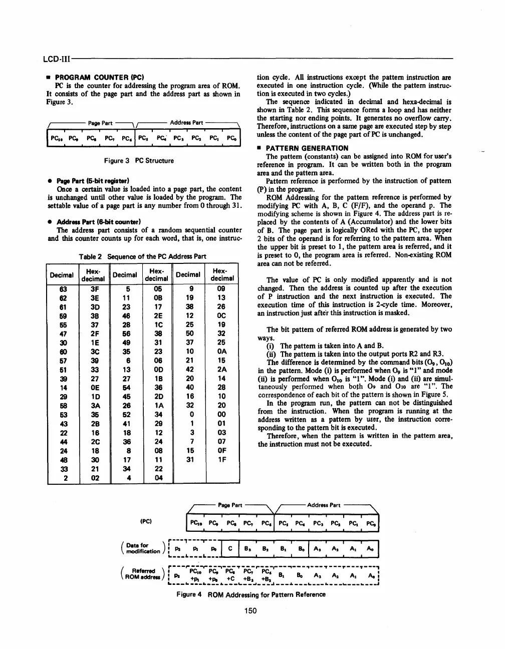
ROM
Addressing for the pattern reference is performed
by
modifying
PC
with
A, B, C
(F/F),
and the operand p. The
modifying scheme
is
shown in Figure 4. The address part is re-
placed
by
the contents
of
A (Accumulator) and the lower bits
of
B.
The page part is logically ORed with
the
PC, the upper
2 bits
of
the operand is for referring
to
the pattern area. When
the upper bit is preset
to
1, the pattern area is referred, and
it
is preset
to
0,
the program area is referred. Non-existing
ROM
area can
not
be referred.
The value
of
PC
is only modified apparently and
is
not
changed. Then the address is counted
up
after the execution
of
P instruction and the next instruction is executed. The
execution time
of
this instruction is 2-cycle time. Moreover,
an instruction just afte'r this instruction is masked.
The
bit
pattern
of
referred
ROM
address is generated
by
two
ways.
(i) The pattern
is
taken
into
A and
B.
(ii)
The pattern is taken
into
the
output
ports R2 and R3.
The difference is determined
by
the command bits
(0
9
, 0
10
)
in the pattern. Mode (i) is performed when
~
is
"1"
and mode
(ii)
is performed when 0
10
is
"1".
Mode
(i)
and (ij) are simul-
taneously performed when
both
09
and 010 are
"1".
The
correspondence
of
each bit
of
the pattern
is
shown in Figure
5.
In
the program run, the pattern can
not
be distinguished
from the instruction. When the program is running
at
the
address written
as
a pattern
by
user, the instruction corre-
sponding
to
the pattern
bit
is executed.
Therefore, when the pattern is written in the pattern area,
the instruction must
not
be executed.
(
Referred
r-
-
-,..
PC::-
pc,-'-
PC:'"
-pC;
"'PC;'-
--
..,--
-
..
-
--.,.
---,.--
-T---1
ROM
address)
: PI +Pt
+p.
+C +BI
+B2
BI
Bo
AI
A2
Al
Ao
I
L
___
~
___
•
___
~
___
~
__
~
___
~
___
~
___
~
___
~
_______
~
___
,
Figure
4 ROM
Addressing
for
Pattern
Reference
150
 Loading...

