---------------------------------LCO-III
Rso.
Ru
G
w
...J
W
U)
:IE
c{
a:
>
c{
...J
a-
U)
i5
DISPLAY
COUNTER &
CONTROL
CIRCUIT
R..
X. Y
C!)
Z
~
1---'----"1..1
w
t-
......
---,/I
~
c
c{
S1
BUS
S2
BUS
RAM
SERIAL
DATA
ALTERNATING
SIGNAL
(M)
SERIAL
SEGMENT
DATA
(D)
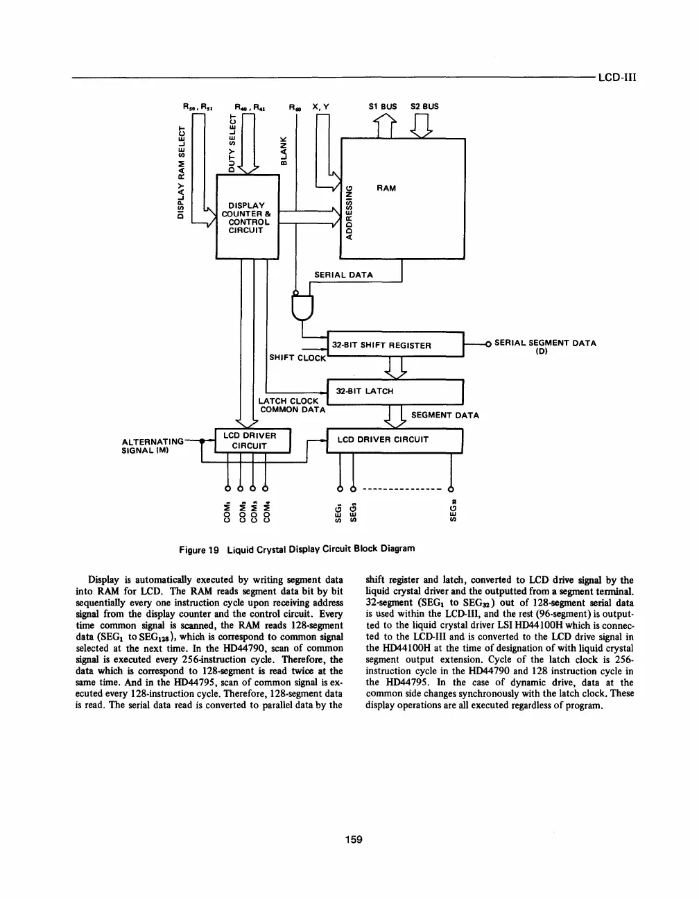
Figure 19 Liquid Crystal Display Circuit Block Diagram
Display
is
automatically executed by writing segment data
into
RAM
for LCD. The
RAM
reads segment data bit
by
bit
sequentially every one instruction cycle upon receiving address
signal from the display counter and the control circuit. Every
time common signal
is
scanned, the
RAM
reads 128-segment
data
(SEG
1
to
SEG
12
8),
which
is
correspond
to
common signal
selected at the next time. In the
HD44790, scan
of
common
signal
is
executed every 256-instruction cycle. Therefore, the
data which
is
correspond
to
128-segment
is
read twice at the
same
time. And in the HD44795, scan
of
common signal
is
ex-
ecuted every 128-instruction cycle. Therefore, 128-segment data
is
read. The serial data read
is
converted to parallel data by the
159
shift register and latch, converted
to
LCD
drive signal by the
liqUid
crystal driver and the outputted from a segment terminal.
32-segment
(SEG
1
to SEG
n
)
out
of
128-segment serial data
is
used within the LCD-III, and the rest (96-segment)
is
output·
ted to the liquid crystal driver
LSI HD44100H which
is
connec-
ted to the LCD-III and
is
converted
to
the
LCD
drive signal in
the
HD44100H at the time
of
deSignation
of
with liquid crystal
segment output extension. Cycle
of
the latch clock
is
256-
instruction cycle in the
HD44790 and 128 instruction cycle
in
the HD44795.
In
the
case
of
dynamic drive, data at the
common side changes synchronously with the latch clock. These
display operations are
all
executed regardless
of
program.
 Loading...

