HMCS44C,HMCS44CL------------------------------------------------------
•
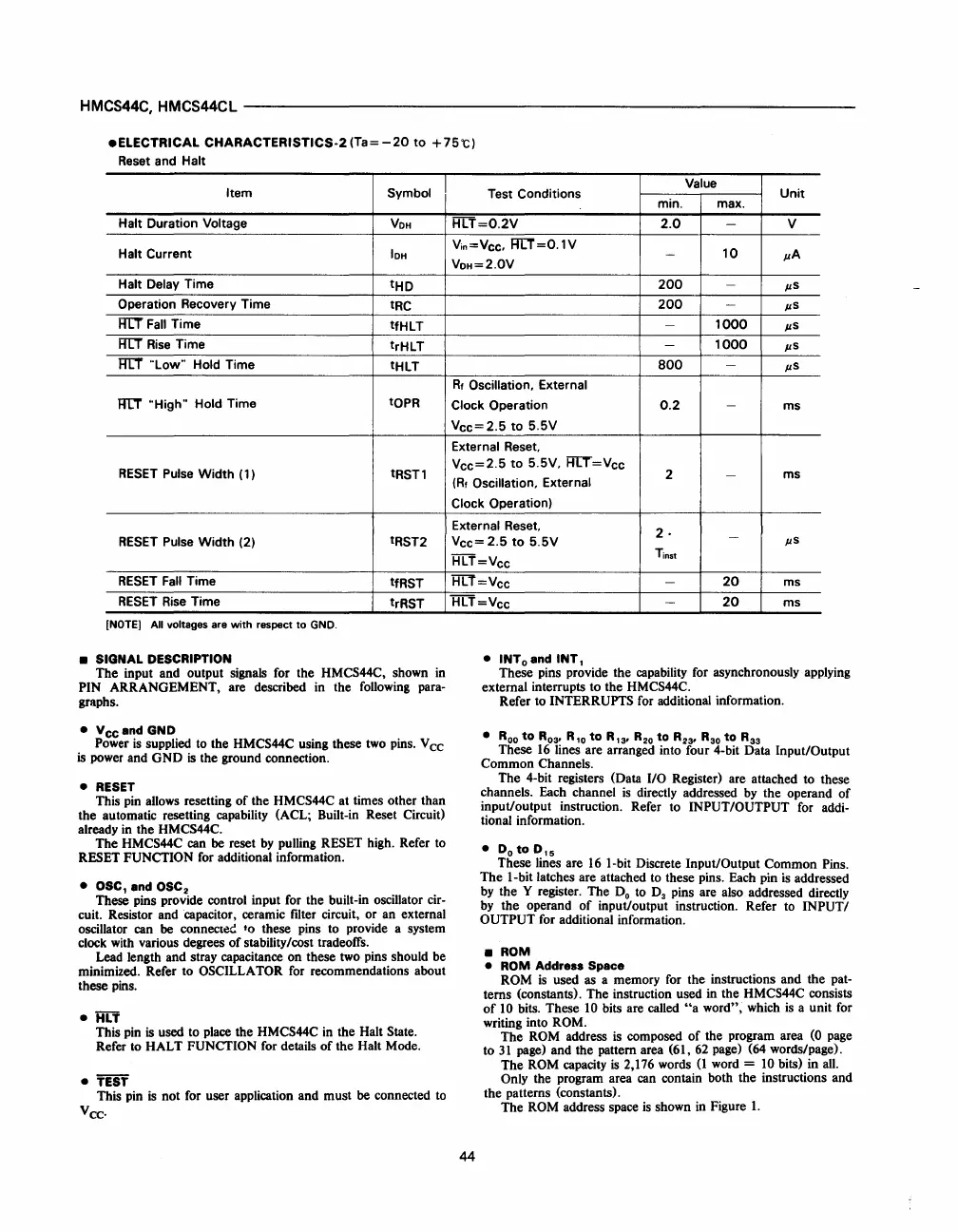
ELECTRICAL
CHARACTERISTICS-2
(Ta
= -
20
to
+ 7 5
"C)
Reset
and Halt
Item
Symbol
Halt
Duration Voltage
VOH
Halt Current
IOH
Halt Delay Time
tHD
Operation Recovery Time
tRC
RITFall
Time
tfHLT
Ff[T
Rise
Time
trHLT
RIT
"Low"
Hold Time
tHLT
RlT "High" Hold Time
tOPR
RESET
Pulse
Width
(1)
tRsn
RESET
Pulse
Width
(2)
tRST2
RESET
Fall
Time
tfRST
RESET
Rise
Time
trRST
[NOTE)
All voltages are
with
respect
to
GND.
• SIGNAL DESCRIPTION
The
input and output signals for the HMCS44C, shown
in
PIN ARRANGEMENT, are described in the following para-
graphs.
• Vcc and GND.
.,
Power
is
supplied to the HMCS44C usmg these two pms.
Vee
is power and
GND
is
the ground connection.
• RESET
This pin allows resetting
of
the HMCS44C at times other than
the automatic resetting capability (ACL; Built-in Reset Circuit)
already in the
HMCS44C,
The
HMCS44C can be reset
by
pulling RESET high. Refer to
RESET FUNCTION for additional information.
• OSC, and OSC
2
These pins provide control input for the built-in oscillator cir-
cuit. Resistor and capacitor , ceramic filter circuit, or an external
oscillator can be connecteG to these pins to provide a system
clock with various degrees
of
stability/cost tradeoffs.
Lead length and stray capacitance on these two pins should be
minimized. Refer to
OSCILLATOR for recommendations about
these pins.
•
HLT
This pin
is
used to place the HMCS44C in the Halt State.
Refer to HALT FUNCTION for details
of
the Halt Mode.
•
TEST
This pin
is
not for user application and must be connected to
Vee·
Value
Unit
Test Conditions
min. max.
HLT=0.2V
2.0
V
Vin=Vcc,
RIT=0.1V
10
/-I
A
-
VOH=2.0V
200
-
/-IS
200
/-Is
-
1000
/-Is
-
1000
/-IS
800
/-IS
Rf
Oscillation, External
Clock Operation
0.2
-
ms
Vcc=
2.5
to
5.5V
External Reset.
Vcc=2.5
to
5.5V,
RIT=Vcc
2
-
(Rf
Oscillation, External
ms
Clock Operation)
External
Reset.
2·
Vcc=
2.5
to
5.5V
-
/-IS
HLT=V
cc
Tinsl
HLi=vcc
-
20
ms
HLT=Vc
c
-
20
ms
44
• INTo and
INT,
.
These pins provide the capability for asynchronously applymg
external interrupts to the
HMCS44C.
Refer to INTERRUPTS for additional information.
•
Roo
to
R
o3
' R,o
to
R'3'
R
20
to
R
23
,
R30
to
R33
These
16
lines are arranged into four 4-bit Data Input/Output
Common Channels.
The 4-bit registers (Data I/O Register) are attached to these
channels. Each channel
is
directly addressed
by
the operand
of
input/output instruction. Refer to INPUT/OUTPUT for addi-
tional information.
• D
o
toD'5
These lines are 16 I-bit Discrete Input/Output Common Pins.
The
I-bit latches are attached to these pins. Each pin
is
addressed
by
the Y register. The
Do
to 0
3
pins are also addressed directly
by
the operand
of
input/output instruction. Refer to INPUT/
OUTPUT
for additional information.
• ROM
• ROM
Address Space
ROM
is
used as a memory for the instructions and the pat-
terns (constants). The instruction used in the HMCS44C consists
of
10 bits. These 10 bits are called
"a
word", which is a unit for
writing into
ROM.
The
ROM address is composed
of
the program area (0 page
to
31
page) and the pattern area (61,
62
page) (64 words/page).
The
ROM capacity
is
2,176 words
(1
word = 10 bits) in all.
Only the program area can contain both the instructions and
the patterns (constants).
The
ROM address space
is
shown in Figure
1.
 Loading...

