HMCS45C,HMCS45CL-------------------------------------------------------
• ELECTRICAL
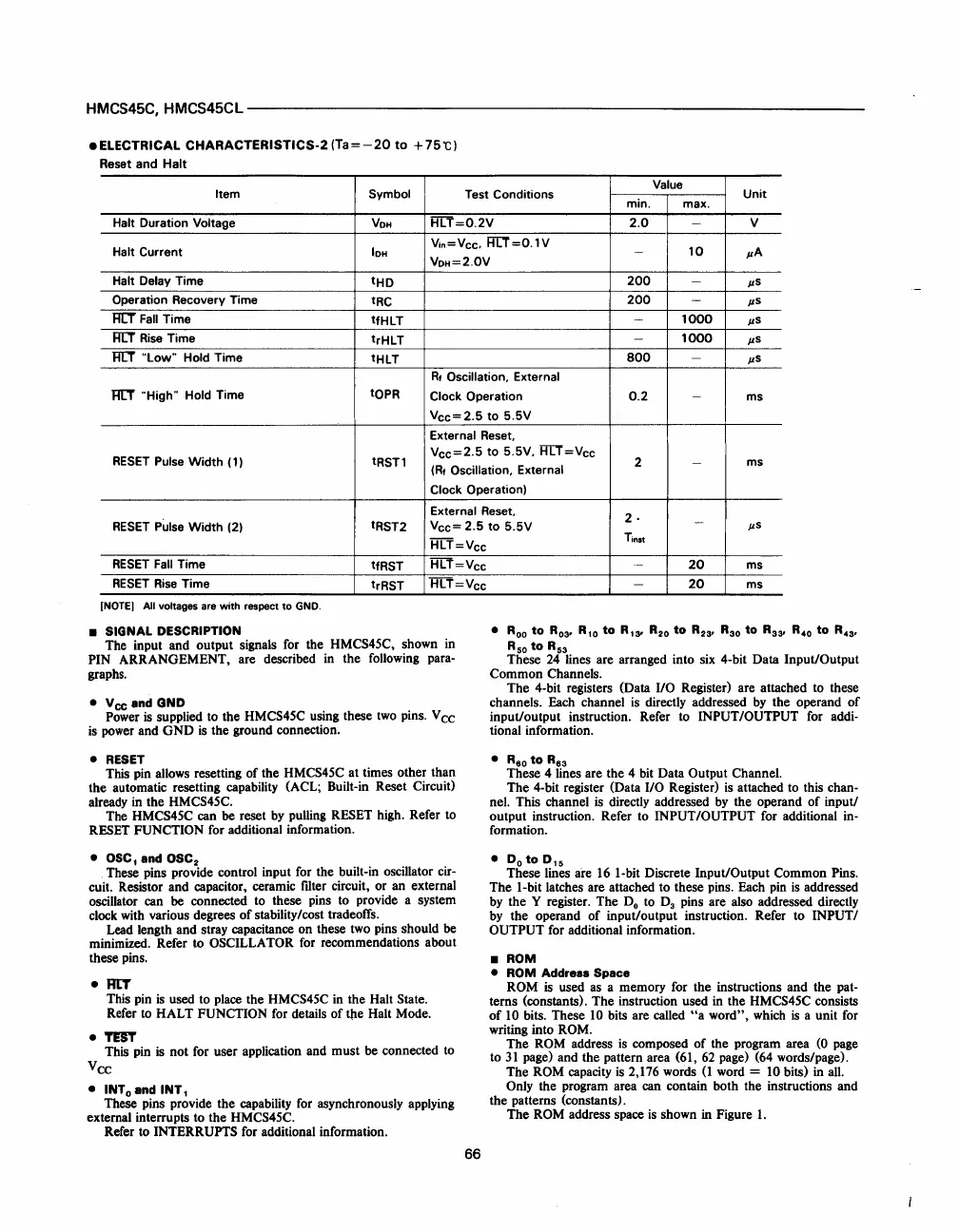
CHARACTERISTICS-2
(Ta
= -
20
to
+
75
'C)
Reset
and
Halt
Value
Item Symbol
Test Conditions
Unit
min.
max.
Halt
Duration Voltage
VOH
HlT=0.2V
2.0
-
V
Halt
Current
IOH
Vin=Vcc,
RIT=0.1V
10
JlA
-
VOH=2.0V
Halt
Delay Time
tHD
200
-
JlS
Operation Recovery Time
tRC
200
-
JlS
RIT
Fall
Time
tfHlT
-
1000
JlS
RIT
Rise
Time
trHlT
-
1000
Jls
RIT
"low"
Hold
Time
tHLT
800
-
JlS
Rt
Oscillation, External
RIT
"High"
Hold
Time
tOPR
Clock
Operation
0.2
-
ms
Vcc=2.5
to 5.5V
External
Reset,
RESET
Pulse Width
(1)
tRST1
Vcc=2.5
to 5.5V,
HIT=V
cc
2
-
(Rt Oscillation, External
ms
Clock Operation)
External
Reset,
2·
RESET
Pulse Width
(2)
tRST2
Vee
= 2.5 to 5.5V
-
JlS
HlT=V
cc
RESET
Fall
Time
tfRST
Hli=vcc
RESET
Rise
Time
trRST
HlT=Vcc
[NOTE)
All voltages are with respect
to
GND.
• SIGNAL DESCRIPTION
The input and output signals for the HMCS45C, shown in
PIN ARRANGEMENT, are described in the following
para-
graphs.
• Vee and GND
Power
is
supplied to the HMCS45C using these
two
pins. Vee
is
power and
GND
is
the ground connection.
•
RESET
This pin allows resetting
of
the HMCS45C at times other than
the automatic resetting capability (ACL; Built-in Reset Circuit)
already in the HMCS45C.
The
HMCS45C can be reset
by
pulling RESET high. Refer to
RESET
FUNCTION for additional information.
•
OSC
I
and OSC
2
These pins provide control input for the built-in oscillator cir-
cuit. Resistor and capacitor, ceramic filter circuit, or an external
oscillator can
be connected to these pins to provide a system
clock with various degrees
of
stability/cost tradeoffs.
Lead length and stray capacitance on these two pins should be
minimized. Refer to
OSCILLATOR for recommendations about
these pins.
•
RtT
This pin
is
used to place the HMCS45C
in
the Halt State.
Refer
to
HALT FUNCTION for details
of
tpe Halt Mode.
•
TRT
This pin
is
not for user application and must be connected
to
Vee
• INTo and
INT
I
These pins provide the capability for asynchronously applying
external interrupts to the HMCS45C.
Refer to
INTERRUPTS for additional information.
66
Tins,
.-
20
ms
-
20
ms
•
Roo
to
R
03
'
RIO
to
R,3' R
20
to
R
23
•
R30
to
R33'
R
40
to
R
43
•
R50
to
R53
These
24
lines are arranged into six 4-bit Data Input/Output
Common Channels.
The 4-bit registers (Data
I/O Register) are attached to these
channels. Each channel
is
directly addressed
by
the operand
of
input/output instruction. Refer to INPUT/OUTPUT for addi-
tional information.
•
R60
to
R63
These 4 lines are the 4 bit Data Output Channel.
The 4-bit register (Data
I/O Register)
is
attached to this chan-
nel. This channel
is
directly addressed
by
the operand
of
input/
output instruction. Refer to
INPUT/OUTPUT for additional in-
formation.
•
Do
to
D
'5
These lines are
16
I-bit Discrete Input/Output Common Pins.
The I-bit latches are attached to these pins. Each
pin
is
addressed
by
the Y register. The
Do
to 0
3
pins are also addressed directly
by
the operand
of
input/output instruction. Refer to INPUT/
OUTPUT for additional information.
• ROM
• ROM
Address Space
ROM
is
used
as
a memory for the instructions and the pat-
terns (constants). The instruction used in the HMCS45C consists
of
10
bits. These
10
bits are called
"a
word", which
is
a unit for
writing into
ROM .
The
ROM address
is
composed
of
the program area (0 page
to
31
page) and the pattern area (61,
62
page) (64 words/page).
The
ROM capacity
is
2,176 words
(1
word = 10 bits)
in
all.
Only the program area can contain both the instructions and
the patterns (constants).
The
ROM address space
is
shown in Figure
1.
 Loading...

