Do you have a question about the HiTech Global HTG-ZRF8 and is the answer not in the manual?
Visual representation of FPGA I/O bank assignments and associated signals.
High-level diagram showing system components and their interconnections.
Diagram illustrating the clock generation and distribution pathways on the platform.
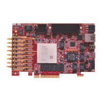
Shows the physical dimensions and layout of the HTG-ZRF8 board.
Details the PCI Express clock circuit and its jitter attenuator.
Circuit diagram showing the logic for enabling the PCI Express clock.
Diagram showing the pinout grid labeling for the FMC+ connector.
Details FMC+ clock generation and adjustable voltage (VADJ) configuration.
Diagram showing clock connections for ADC and DAC interfaces.
Procedure for booting from Quad-SPI flash memory.
Procedure for booting the device from an SD card.
| Brand | HiTech Global |
|---|---|
| Model | HTG-ZRF8 |
| Category | Motherboard |
| Language | English |