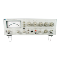
Model 339A
Section
VIII
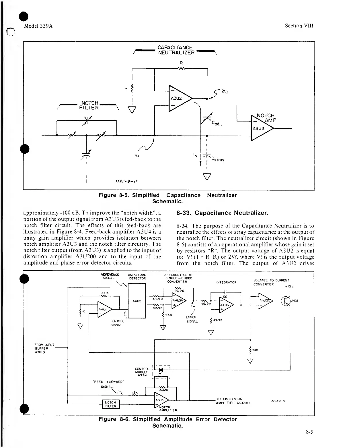
Figure
8-5.
Simplified
Capacitance
Neutralizer
Schematic.
approximately
-100
dB.
To
improve
the ’'notch width",
a 8-33.
Capacitance
Neutralizer,
portion
of
the
output signal from
A3U3 is fed-back to the
notch filter circuit. The effects of this
feed-back are
8-34.
The
purpose of the Capacitance Neutralizer is to
illustrated in
Figure
8-4.
Feed-back
amplifier A3U4 is
a
neutralize the effects of
stray capacitance
at the output of
unity gain
amplifier which provides
isolation between
the notch filter. The
neutralizer
circuit
(shown
in Figure
notch
amplifier
A3U3 and
the
notch filter circuitry.
The
8-5)
consists of an operational amplifier whose gain is
set
notch filter
output
(from A3U3) is applied to the input
of
bv
resistors “R". The output
voltage
of A3U2 is equal
distortion amplifier A3U200 and to the input
of the
to:
Vf(l
+
R R)
or
2Vf,
where Vf is
the output
voltage
amplitude and phase error detector circuits.
from the notch
filter. The output
of A3U2 drives
FROM
INPUT
BUFFER
A3UIOI
REFERENCE
AMPLITUDE DIFFERENTIAL
TO
AMPLIFIER
Figure 8-6.
Simplified
Amplitude Error Detector
Schematic.
8-5