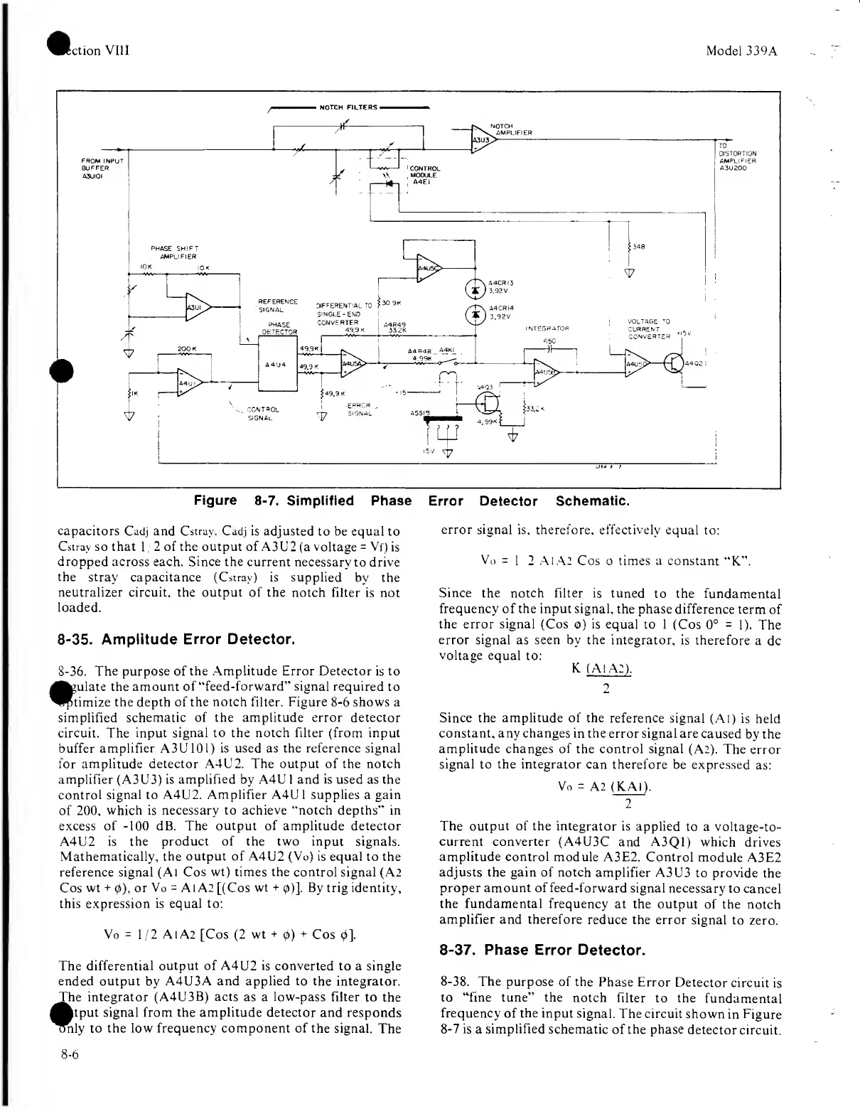
Figure
8-7.
Simplified Phase
Error
Detector
Schematic.
capacitors
Cadj and
Cstrav.
Cadj is adjusted to be
equal to
Cstray
so
that
1 2 of the
output
of A3U2
(a
voltage
=
Vf)
is
dropped across each. Since the
current necessary
to
drive
the stray capacitance (Cstray)
is supplied
by the
neutralizer circuit, the output of the
notch filter is
not
loaded.
8-35.
Amplitude
Error Detector.
8-36.
The
purpose
of
the Amplitude Error Detector
is
to
dfcgulate the amount
of “feed-forward” signal required
to
^^timize the depth of
the notch
filter.
Figure
8-6
shows
a
simplified
schematic of
the
amplitude error detector
circuit. The
input signal to the notch filter (from input
buffer
amplifier
A3 U
101)
is used as the reference signal
for
amplitude detector A4U2. The
output
of the notch
amplifier (A3U3) is
amplified
by A4U I and
is
used as the
control signal to A4U2.
Amplifier
A4U 1
supplies
a gain
of
200,
which is necessary to
achieve
“notch depths” in
excess of
-100
dB.
The output of
amplitude detector
A4U2
is the product of the two input signals.
Mathematically,
the output of A4U2 (Vo) is equal
to
the
reference signal (Al
Cos wt) times the control
signal (A2
Cos wt
+
0),
or
Vo
=
Al
A2 [(Cos
wt
+
0)].
By
trig identity,
this expression
is equal to:
Vo
=
1/2
A
i
A2
[Cos
(2
wt
+
0)
+
Cos
0],
The
differential output of A4U2 is converted
to a single
ended output
by
A4U3A and applied to the integrator.
The integrator
(A4U3B) acts
as a
low-pass
Filter to the
^vput
signal from the
amplitude
detector and
responds
only to the low frequency component of the signal.
The
error signal
is. therefore, effectively equal
to:
Vo
=
1 2
AI.A2
Cos o times a constant
“K”.
Since
the notch Filter is tuned
to the
fundamental
frequency of the input signal,
the phase difference
term
of
the error signal (Cos
0)
is
equal to
1
(Cos
0°
=
1).
The
error signal
as seen by
the
integrator, is
therefore
a
dc
voltage
equal to:
K
(Al
A2),
2
Since the amplitude of the
reference signal
(Al) is
held
constant, any changes in the
error signal are
caused
by the
amplitude changes of
the control signal
(
A2).
The
error
signal to the integrator
can therefore be expressed
as:
Vo
=
A2
(K.AI)
.
2
The output of the integrator
is applied to
a voltage-to-
current
converter
(A4U3C and A3Q1)
which
drives
amplitude control module
A3E2. Control
module
A3E2
adjusts the gain of notch
amplifier A3U3
to provide
the
proper amount of feed-forward
signal necessary
to cancel
the fundamental frequency
at the output
of the notch
amplifier and therefore reduce
the error
signal to
zero.
8-37.
Phase Error
Detector.
8-38.
The
purpose of the
Phase Error
Detector
circuit
is
to “fine tune” the
notch filter to
the
fundamental
frequency
of
the input
signal.
The circuit
shown
in Figure
8-7
is
a
simpliFied
schematic
of
the phase
detector
circuit.
8-6
 Loading...